![]()

Router vs Laser vs V-Cut vs Punching: Which PCB Depaneling Method Fits Your Factory
If you’re standing on the factory floor trying to figure out the best way to separate your latest batch of PCBs, here’s the honest truth: there’s no such thing as a ‘perfect’ method. It all comes down to your specific production volume and how much ‘real estate’ you’re working with on the board. Let’s break down what actually fits your workflow.
To put it simply:
- Choose V-Cut for high-volume, straight-edged boards where cost is the main driver.
- Choose Punching if you are stamping out millions of identical, simple boards and can absorb the high upfront tooling costs.
- Choose an advanced pcb router machine for high-mix production requiring complex shapes and medium-to-high volumes.
- Choose a pcb laser cutting machine if you are working with High-Density Interconnect (HDI) boards, sensitive MLCCs, or flex circuits where mechanical stress must be absolute zero.
As solutions experts who have optimized dozens of SMT (Surface Mount Technology) lines, we’ve seen the devastating effects of choosing the wrong method—cracked components, endless manual deburring, and high scrap rates. According to industry data, improper depaneling can lead to failure rates as high as 5-10% in sensitive applications.
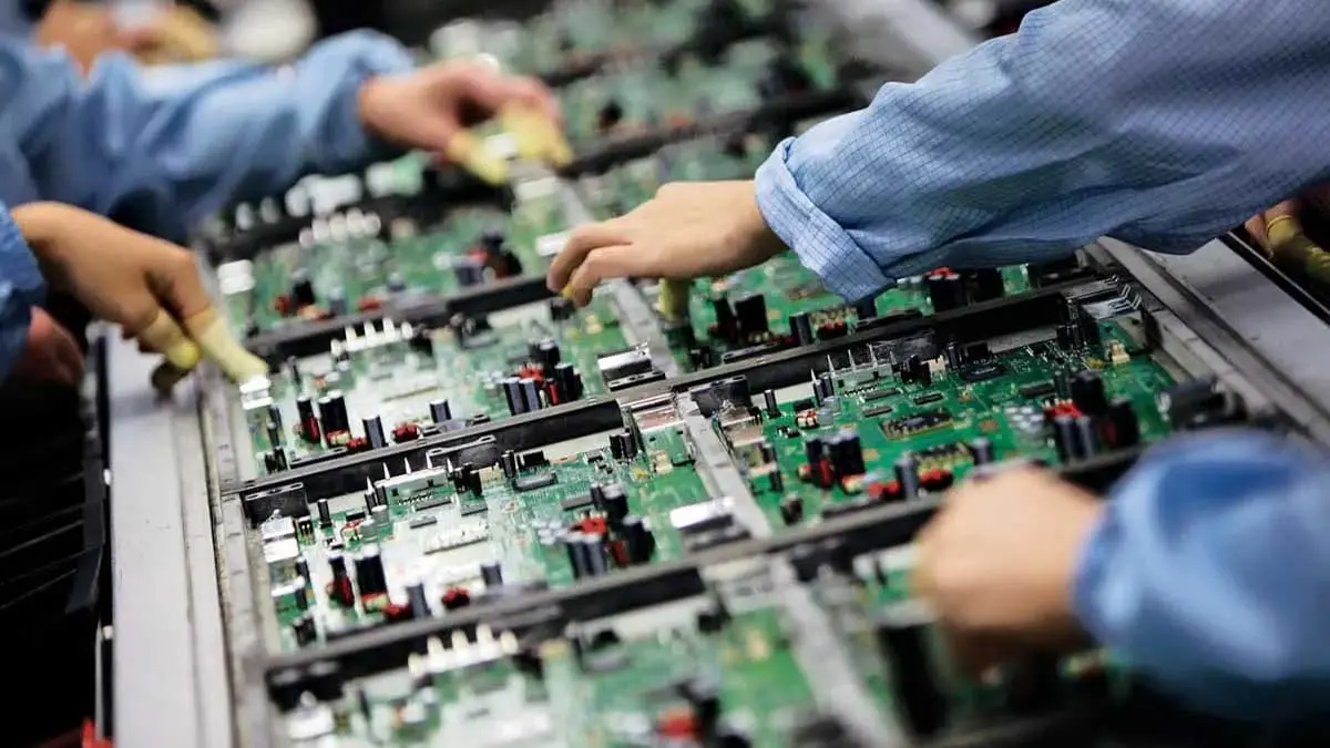
Implementing the right separation technology immediately benefits your factory by drastically lowering your defect rate, boosting your Units Per Hour (UPH), and completely eliminating catastrophic field failures caused by mechanical stress. Let’s break down the engineering reality of each method and how to start making the right choice.
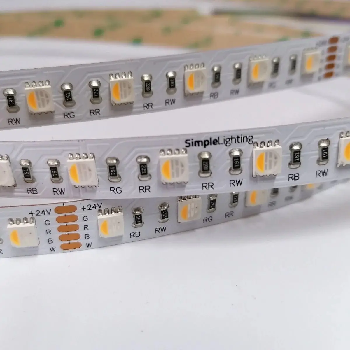
1. V-Cut (V-Scoring) Depaneling: The High-Volume Workhorse
V-scoring is one of the oldest and most widely used separation techniques on the market. During board fabrication, a V-shaped groove is cut into the top and bottom of the panel, leaving a thin web of FR-4 material holding the boards together. After assembly, a machine with circular blades rolls along these grooves to snap the boards apart.
How it Works:
Circular cutting blades shear the remaining web of material along the pre-scored straight lines.
The Benefits:
It is incredibly fast, very cost-effective per board, and requires zero custom tooling. Because it uses a rolling blade, the operation is straightforward, and the machine itself requires very little maintenance compared to CNC systems.
The Downside:
V-cut is strictly limited to straight-line separations. You cannot cut curves or complex geometries. Additionally, it requires a significant “keep-out” zone for components, as the mechanical snapping generates moderate to high bending stress.
When to Use It:
We highly recommend V-Cut for low-complexity, high-volume rectangular boards like LED light strips, basic power supplies, or simple consumer electronics. However, if your boards are highly dense, you will need to look into v-cut depaneling alternatives to protect your yield.
2. Punching (Die-Cutting): The Mass-Production Giant
Punching uses a custom-machined metal die to stamp individual PCBs out of a larger panel in a single, powerful press stroke.
How it Works:
The panel is loaded into a press, and a heavy mechanical die punches out the board outline instantly.
The Benefits:
Speed. Nothing beats punching for pure throughput. It leaves minimal debris and can process highly complex shapes instantly. For the right product, punching provides a massive output rate that routing simply cannot match.
The Downside:
The initial tooling cost for the custom die is extremely high. If your PCB layout changes by even a millimeter, the die is useless, and you must buy a new one. Furthermore, the massive physical force of the press can send shockwaves through rigid substrates, making it risky for delicate solder joints.
When to Use It:
Ultra-high volume manufacturing (over 50,000 units per month) where the board design is 100% locked in. It is widely used in the automotive sector for simple sensor boards and separating thin Flexible Printed Circuits (FPCs).
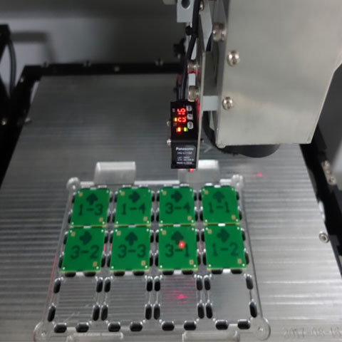
3. Router (Tab Routing): The Flexible All-Rounder
If your boards have irregular shapes, curved edges, or overhanging connectors, you need CNC routing. During panel design, the individual boards are held together by small “tabs” or “mouse bites” that the router mills away.
How it Works:
A high-speed spindle uses a carbide bit to mill through the FR-4 tabs. Typical cutting speeds range from 50 to 100 mm/s depending on material thickness.
The Benefits:
Immense flexibility. It can cut any geometric shape. When parameters are properly optimized, a rigidly fixtured router produces very clean edges, and there is no need to buy expensive custom dies for every new board design.
The Downside:
Mechanical routing generates fiberglass dust that requires heavy vacuum extraction. It also causes micro-vibrations. To avoid long-term reliability issues on components, process engineers must carefully monitor spindle speeds. As the router bit wears down, the stress it puts on the board increases significantly.
When to Use It:
High-mix, medium-to-high volume production with complex board outlines. To eliminate human handling errors, we always advise our clients to integrate this process into fully automated pcb depaneling solutions with robotic loading and unloading.
4. Laser Depaneling: The Zero-Stress Future
For modern electronics—think wearables, medical devices, and automotive sensors—components are packed so tightly that even the vibration of a standard router bit is unacceptable. Laser depaneling uses a highly focused beam of light to vaporize the material without ever touching it.
How it Works:
A UV or Green laser performs “cold ablation,” breaking the molecular bonds of the substrate layer by layer without generating massive heat or physical force.
The Benefits:
True zero mechanical stress. A comprehensive industry analysis found that approximately 12% of PCB assembly defects trace back to mechanical stress during depaneling. Lasers fix this completely. In fact, leading capacitor manufacturers recommend keeping mechanical strain below 500 µstrain. While mechanical routers often spike above 800-1000 µstrain as bits dull, a laser system consistently keeps stress below 50 µstrain. This completely eliminates the risk of cracking delicate MLCCs (ceramic capacitors) or BGA joints.
The Downside:
Higher initial equipment cost and slightly slower cutting speeds for very thick FR-4 boards (e.g., above 2.0mm) compared to V-cut.
When to Use It:
HDI boards, rigid-flex circuits, strict medical applications, and any design where components are placed within 1.0mm of the board edge. If you are serious about yield, upgrading to a pcb laser cutting machine pays for itself rapidly by destroying your scrap rate.
Best Practices: How to Optimize Your Separation Process
Selecting the machine is only half the battle. How you deploy it determines your actual ROI. Here are the engineering best practices we enforce on the floor when consulting for our clients.
Practice 1: Kerf Math to Boost Panel Yield
If you are transitioning from routing to laser, you need to redesign your panels to take advantage of the technology. A mechanical router requires a physical channel (kerf) of about 2.0mm to 3.0mm to allow the bit to pass through.
The Result:
A laser beam has a microscopic kerf width of only 20 to 50 micrometers. By reducing the required spacing between boards from 3.0mm down to 0.2mm, you can pack boards closer together. Moving from routing to laser cutting commonly increases overall panel yield by 15% to 30%, saving massive amounts of raw FR-4 material over a year.
Practice 2: Automate for Cycle Time Reduction
Manual loading and unloading of panels introduces alignment errors, drops throughput, and creates a massive bottleneck right at the end of your SMT line.
The Result:
One thing we always tell our clients: Let your IPC Class dictate your cutting method. Not every board needs the same level of precision. If you’re building Class 3 mission-critical electronics—like medical or aerospace gear—you can’t afford the micro-cracks or stress that come with mechanical routing. You need the precision of a laser. But if it’s a simple Class 1 consumer toy, a traditional V-cut might be the most cost-effective way to get the job done.
Practice 3: Match the Method to the IPC Class
Do not over-engineer or under-engineer your process based on cost alone; base it on reliability requirements.
The Result:
If you are manufacturing IPC Class 1 consumer electronics, standard V-Cut or Routing is perfectly fine. However, if you are producing IPC Class 3 (High Reliability) or medical devices, mechanical routing is often a liability. For these high-stakes environments, laser depaneling is frequently specified directly in procurement requirements because the traceability and zero-stress guarantees are non-negotiable.
Data-Driven Comparison: Which Method Wins?
To summarize the technical metrics for process engineers, here is how the four technologies stack up against each other on the factory floor:
| Process Metric | V-Cut Depaneling | Punching (Die-Cut) | Mesin Penghala PCB | PCB Laser Cutting Machine |
| Component Stress | Moderate to High | Low to Moderate | Moderate (<200 µstrain) | Zero (<50 µstrain) |
| Edge Quality | Rough & Fibrous | Clean but can have burrs | Smooth | Perfect, sealed edge |
| Kerf Width Waste | None (Pre-scored) | N/A | High (2.0mm – 3.0mm) | Lowest (0.02 – 0.05mm) |
| Tooling Cost | Low | Very High (Custom Dies) | Medium (Bit replacement) | Low (No physical bits) |
| Shape Flexibility | Straight Lines Only | Any shape (if die allows) | High (Any geometry) | Highest (CAD driven) |
Frequently Asked Questions (FAQ)
1. Is V-Cut cheaper than router depaneling?
Yes, for straight-line cuts. V-scoring requires no consumable router bits and no complex vacuum dust extraction systems. However, its major limitation is that it cannot cut curves or 90-degree internal corners, making it entirely unsuitable for complex board shapes.
2. How much clearance do I need to leave between components and the cutting edge?
It really comes down to the mechanical stress involved.
For traditional Routing or V-Scoring: You usually need a “safety buffer” of 2.0mm to 3.0mm. Anything closer puts your delicate components at risk of micro-cracking due to the vibrations and physical force of the blade.
For Laser Depaneling: Since it’s a zero-stress, non-contact process, those restrictions pretty much disappear. You can safely pack your components as close as 0.5mm to the edge.
3. Does punching cause damage to the PCB?
Punching is fast, but the immense mechanical force of the die can send shockwaves through rigid FR-4 substrates. While it is excellent for flexible circuits (FPCs), using it on rigid boards populated with brittle components requires highly optimized die designs to prevent solder joint fracturing.
4. Can a laser cutting machine process thick FR-4 boards?
Yes, modern high-power lasers (such as 35W Green lasers) can cleanly cut standard 1.6mm and even 2.0mm FR-4 boards. While it may be slightly slower than a high-speed router on very thick boards, the tradeoff is a perfectly clean, burr-free edge with absolute zero component stress.
5. How do I know if routing vibration is damaging my boards?
Invisible mechanical stress often manifests as field failures weeks after the product has shipped. If you suspect routing damage, you should attach strain gauges to your boards near the cut lines. If the measured stress exceeds 200 microstrain, your router feed rate is too aggressive, your bit is dull, or you need to switch to a non-contact laser method to protect your yield.