![]()

PCB Router Machine for Thick PCBs: Solve Vibration and Burr Issues in Mass Production
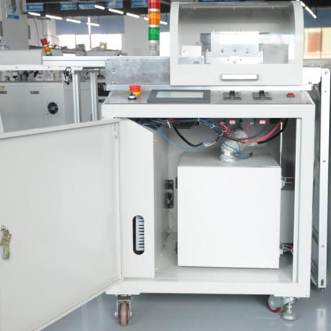
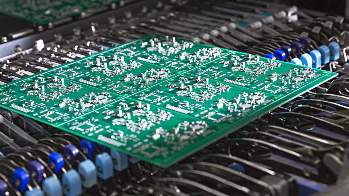
Are you running a mass production line, struggling to depanel thick FR-4 boards without leaving jagged fiberglass burrs or vibrating your BGA components to failure? If you clicked on this guide searching for the perfect router settings, we are going to give you the direct, field-tested answer right now: while an advanced pcb router machine with heavy vacuum fixturing can mitigate some of these defects, the ultimate, permanent solution to eliminate both vibration and burrs on thick, high-density boards is upgrading to a pcb laser cutting machine.
In our years of optimizing EMS (Electronic Manufacturing Services) factory floors, we have watched process engineers waste countless hours tweaking feed rates and changing expensive carbide router bits trying to cleanly cut 1.6mm or 2.4mm heavy-copper boards. The harsh reality is that mechanical routing on thick substrates inherently generates friction and mechanical stress. By transitioning to a non-contact laser process, you achieve absolute zero mechanical vibration, flawless burr-free edges, and massive material savings.
Let’s dive into the physics of why your thick PCBs are suffering, why manual deburring is destroying your ROI, and how you can start implementing laser technology to solve these mass production nightmares once and for all.
The Physics of Failure: Why Thick PCBs Hate Mechanical Routing
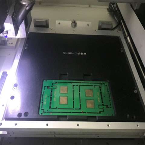
When we consult for high-volume automotive and industrial electronics manufacturers, we constantly see the same fundamental misunderstanding: treating a thick 2.0mm FR-4 board the same as a thin 0.8mm consumer board. Increasing the thickness of the FR-4 material vastly increases its mechanical strength, allowing the PCB to withstand higher bending forces. However, this exact rigidity is what makes mechanical depaneling so destructive.
When you plunge a physical cutting tool into a dense, thick substrate, two massive enemies emerge on your SMT line: Vibration and Burrs.
1. The Anatomy of a Burr
In real production, burrs are tiny fiberglass or resin fibers, or micro copper protrusions left along the board edge. Milling is a mechanical shearing process; as long as your router bit is brand new and razor-sharp, it cuts cleanly. But cutting thick FR-4—especially multi-layer boards with heavy copper—destroys carbide bits incredibly fast. As the bit dulls, it stops smoothly slicing the glass fibers and starts violently tearing them. This tearing action is what leaves the rough, jagged burrs that fail strict quality control audits.
2. The Micro-Vibration Epidemic
Vibration is the silent killer of printed circuit board assemblies. Thick boards resist the router bit, and this mechanical resistance pushes back against the spindle. If the board is not clamped perfectly flat, it begins to flutter. This mechanical stress travels directly through the stiff board, creating micro-cracks in delicate components like MLCCs (ceramic capacitors) and BGA solder joints. These latent defects are terrifying because they often pass the factory’s end-of-line electrical testing, only to fail weeks later in the field under thermal cycling or normal operational vibration.
The Hidden Costs of Routing Burrs in High-Volume Assembly
Many factory managers try to solve the burr problem by adding a manual deburring station at the end of the line. We always tell our clients: throwing manual labor at a precision engineering problem destroys your ROI.
If operators are using files or sandpaper to clean up the edges of a thick board, you are introducing several critical risks:
- Contamination and Shorts: The dust and conductive copper swarf created by mechanical routing and manual filing can easily migrate onto the board surface. If a tiny piece of loose copper lands between two fine-pitch component pads, it creates a catastrophic electrical short.
- Enclosure Fitment Failures: In modern electronics, internal space is highly restricted. If a thick board has an oversized outline due to a fiberglass burr, it simply will not slide into its final aluminum or plastic housing.
- Yield Drops: Relying on manual handling to snap or file boards often introduces uneven bending forces across the PCB, heavily spiking your scrap rate.
“Poor depaneling can lead to microcracks, delamination, or component failures during subsequent assembly… selecting the right depaneling method directly impacts compliance with quality benchmarks like IPC-A-600.”
The Ultimate Upgrade: Why a Laser Machine is the Answer
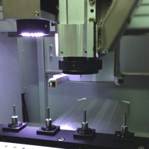
If you want to completely engineer burrs and vibration out of your mass production line, you must remove the mechanical friction. This is why top-tier manufacturers are abandoning the traditional milling cutter pcb depaneling machine in favor of high-power laser systems for dense, high-value thick boards.
1. True Zero-Stress Separation
A laser depaneling system utilizes a focused beam of light (typically UV or Green laser) to vaporize the FR-4 substrate layer by layer. Because no physical tool ever touches the board, there is absolutely zero mechanical strain, zero chatter, and zero vibration transferred to your components. For boards populated with fragile ceramic capacitors placed near the edge, this contactless process is a lifesaver.
2. Flawless, Burr-Free Edges
Lasers do not suffer from tool wear. The 10,000th board cut by a laser will have the exact same edge quality as the 1st board. The ablation process leaves a perfectly clean, sealed edge with absolutely no exposed fiberglass fibers or burrs. You can completely eliminate your secondary manual deburring stations.
3. Cutting Thick Boards with High Power
A common misconception is that lasers can only cut thin flexible circuits (FPC). This is outdated. Modern 35W green light laser cutting machines are specifically engineered to cut thick PCBs, easily achieving a clean processing thickness of up to 2.0mm with impressive efficiency.
4. Massive Material Savings (The Kerf Advantage)
A standard router bit requires a massive 2.0mm to 3.0mm routing channel between individual boards to physically pass through the panel. A laser beam, however, is microscopic. A typical laser kerf is only 20 to 50 micrometers wide. This allows layout designers to push individual boards incredibly close to each other on the manufacturing panel, commonly increasing overall panel material yield by 15% to 30%.
Engineering Best Practices: How to Optimize Your Production
Whether you are transitioning to laser or optimizing your existing CNC setup, how you start the integration dictates your success. Here are the best practices we deploy for our clients.
Practice 1: Reclaim Your Board Real Estate
If you are upgrading to a non-contact laser, you must update your CAD files to take advantage of it. Because there is no mechanical vibration, you no longer need to keep sensitive components 3.0mm away from the cutting edge. You can safely move components to within 0.5mm of the separation line. Redesign your panels to shrink the “keep-out” zones, which immediately lowers your FR-4 material costs per unit.
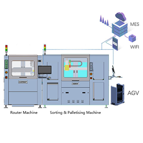
Practice 2: Integrate Inline Automation
To truly maximize the efficiency of mass production, remove human hands from the loading process. We highly recommend pairing your cutting technology with an inline depaneling system. By feeding thick panels straight from the SMT conveyor into the laser cell, and using robotic arms to pick and place the finished boards into output trays, you ensure absolute consistency and prevent handling damage.
Practice 3: Router Optimization (If You Must Route)
If budget constraints mean you must temporarily stick with routing, you must treat your fixture as part of the cutting system. Utilize full-area vacuum fixtures to support the heavy board completely, minimizing flutter. Furthermore, manage your spindle’s “chip load.” Do not just run the spindle at maximum RPM; balance the feed rate and spindle speed to ensure the bit is actually slicing the material, rather than rubbing and burning the resin.
Real-World Data: Laser vs. Mechanical Routing
When justifying the capital expenditure for automated pcb depaneling solutions, the total cost of ownership (TCO) speaks for itself.
| Production Metric | Mechanical Router | PCB Laser Cutting Machine |
| Edge Quality | Prone to burrs as tool wears | Perfectly clean, sealed edge |
| Component Stress | High (Vibration and chatter) | Zero (Non-contact) |
| Consumable Costs | High (Frequent bit replacements) | Zero (No physical tools) |
| Required Kerf Width | 2.0mm – 3.0mm | 0.02mm – 0.05mm |
| Max PCB Thickness | Standard | Up to 2.0mm (with 35W Green Laser) |
By eliminating the cost of replacement router bits, removing the labor hours spent on manual deburring, and recovering up to 30% more usable boards per panel due to the microscopic kerf, the ROI on a laser system for mass production is achieved rapidly.
Kesimpulan
Manufacturing thick, high-density PCBs requires precision that brute-force mechanical tools simply struggle to maintain over thousands of cycles. A dull router bit will inevitably cause vibration, and that vibration will crack your components and leave messy burrs. By understanding these physics and upgrading to a non-contact laser process, you protect your yield, guarantee product reliability in the field, and significantly lower your operational costs. Stop fighting your equipment, and start cutting with light.
Frequently Asked Questions (FAQ)
Q1. Can a laser cutting machine actually handle thick FR-4 boards?
Yes. While UV lasers are often used for thin flexible circuits, high-power lasers—such as 35W green laser systems—are explicitly designed to cleanly cut thick FR-4 boards up to 2.0mm thick without burning the edges.
Q2. Why do thick boards cause more burrs than thin boards during routing?
Thick boards offer much higher mechanical resistance to the router bit. This resistance dulls the carbide flutes very quickly. Once the bit is dull, it no longer cuts the fiberglass cleanly; instead, it tears the resin and copper, leaving behind frayed fibers known as burrs.
Q3. How does laser cutting improve my overall panel yield?
Mechanical routers require a wide physical path (kerf) of about 2.0mm to 3.0mm to separate boards. A laser beam has a kerf of only 20 to 50 micrometers. This massive reduction in wasted space allows you to nest more individual PCBs onto a single panel, directly reducing material costs.
Q4. What is the safe distance to place components from the cutting edge?
If you are using a mechanical router or V-cut machine, industry standards recommend keeping sensitive components (like BGAs or MLCCs) at least 3.0mm away to protect them from mechanical stress. With the zero-stress nature of laser depaneling, components can be placed as close as 0.5mm from the edge.
Q5. How do I stop micro-cracks in my ceramic capacitors during depaneling?
Micro-cracks are caused by the board flexing or vibrating during physical separation. The only way to entirely prevent them is to eliminate mechanical force. Switching to a non-contact laser separation method guarantees that zero bending stress or vibration is transferred to the fragile ceramic bodies.