![]()
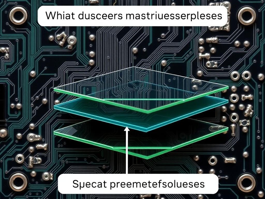
What are separate layers on pcb
Understanding PCB Layers: A Comprehensive Guide to Printed Circuit Board Construction
In today’s rapidly evolving electronics industry, understanding the intricacies of PCB layers is crucial for anyone involved in electronic product manufacturing or PCB design. This comprehensive guide will walk you through everything you need to know about PCB layers, from basic concepts to advanced manufacturing considerations. Whether you’re a seasoned professional at a major electronics company or an individual PCB enthusiast, this article will provide valuable insights into the world of printed circuit board construction.
What Are PCB Layers and Why Are They Important?
PCB layers are the fundamental building blocks that make up a printed circuit board. Each layer serves a specific purpose in the overall functionality and performance of the electronic device. The number of layers in a PCB can range from single-layer designs to complex multilayer configurations, depending on the application requirements.A typical PCB consists of several key layers:
- Copper Layer: The conductive material that carries electrical signals
- Substrate Layer: The base material providing structural support
- Solder Mask: The protective coating that prevents short circuits
- Silkscreen Layer: Contains component markings and identifiers
Types of PCB Layers: From Simple to Complex
Single-Layer PCBs
The most basic type of PCB features one layer of conductive copper on a substrate material. These boards are:
- Cost-effective for simple circuits
- Ideal for basic electronic products
- Limited in complexity and functionality
Double-Layer PCBs
Adding a second copper layer creates more routing possibilities:
- Components can be mounted on both sides
- Increased circuit density
- Better signal integrity
- More complex circuit designs possible
Multilayer PCBs
Modern electronic devices often require multilayer PCB solutions with 4, 6, 8, or more layers:
- Enhanced signal integrity
- Better power distribution
- Reduced electromagnetic interference
- Higher component density
How Do Different PCB Layers Work Together?
The interaction between various PCB layers is crucial for proper circuit function. Here’s how they complement each other:
- Signal Layers
- Carry electrical signals between components
- Usually made of copper
- Can be internal or external
- Power and Ground Layers
- Provide stable power distribution
- Reduce noise and interference
- Improve overall performance
- Dielectric Layers
- Insulate between conductive layers
- Maintain signal integrity
- Prevent short circuits
PCB Layer Stack-Up Design Considerations
When designing PCB layer stack-ups, several factors must be considered:
| Layer Type | Purpose | Common Materials |
|---|---|---|
| Top Layer | Component mounting and routing | Copper |
| Inner Layer 1 | Power distribution | Copper |
| Inner Layer 2 | Ground plane | Copper |
| Bottom Layer | Additional routing | Copper |
Advanced PCB Layer Technologies and Trends
Modern PCB manufacturing has evolved to include:
- High-density interconnect (HDI) technology
- Embedded components
- Flexible and rigid-flex PCBs
- Advanced routing solutions
How to Choose the Right Number of PCB Layers?
Consider these factors when determining layer count:
- Circuit complexity
- Signal integrity requirements
- Cost constraints
- Production volume
- Space limitations
PCB Layer Manufacturing Process
The manufacturing process involves several steps:
- Layer preparation
- Lamination
- Drilling
- Plating
- Etching
- Final separation using advanced depaneling equipment
Common PCB Layer Problems and Solutions
Typical Issues:
- Signal interference
- Impedance mismatches
- Power distribution problems
- Manufacturing defects
Solutions:
- Proper stack-up design
- Advanced materials selection
- Quality control measures
- Professional PCB processing equipment
Frequently Asked Questions
How many layers should my PCB have? The number of layers depends on your specific requirements, but most modern designs use 4-8 layers for optimal performance.What is the maximum number of layers possible in a PCB? While theoretically unlimited, practical PCBs typically max out at 32 layers due to manufacturing constraints and cost considerations.How do I determine the best layer stack-up for my design? Consider factors like signal integrity, power requirements, and cost constraints when planning your layer stack-up.What’s the difference between core and prepreg layers? Core materials are fully cured, while prepreg materials are partially cured and used to bond cores together during lamination.
Key Takeaways
• PCB layers are fundamental to electronic device functionality • Layer count affects performance and cost • Proper stack-up design is crucial for success • Manufacturing quality depends on equipment and processes • Advanced technologies enable more complex designs • Professional PCB processing solutions ensure quality results
