![]()

Punching vs Laser Depaneling for FPC: Choosing the Right Process for Cost and Yield
If you are setting up a surface mount technology (SMT) production line for Flexible Printed Circuits (FPCs)—whether for medical wearables, smartphone camera modules, or automotive displays—you need a definitive answer on how to separate these delicate boards from the manufacturing panel. We will give you the direct answer right from our experience on the factory floor:
Use die punching if you are running massive volumes (over 1 million units annually) of a single, locked-in design where throughput speed and low per-unit cost are your only metrics. Use a pcb laser cutting machine if you are running high-mix production, dealing with High-Density Interconnect (HDI) flex, or if your primary goal is achieving a 99.9% yield rate with absolute zero mechanical stress.
Flexible printed circuits are entirely different beasts compared to standard rigid FR4 boards. You simply cannot run a flex board through traditional manual snapping, and while an advanced pcb router machine works wonders on rigid materials, a spinning mechanical bit will quickly snag and tear the thin polyimide (PI) substrate of a flex circuit. Therefore, the choice almost always boils down to Punching vs. Laser.
In our years as solutions experts, we have seen manufacturing companies bleed money by choosing the wrong method—either by paying thousands of dollars for new punching dies every week for prototyping, or by bottlenecking a mass-production line with outdated equipment. Let’s break down the engineering reality, the hidden costs, and how to start optimizing your FPC yield today.
สารบัญ
The Engineering Challenge: Why FPCs Fail During Depaneling
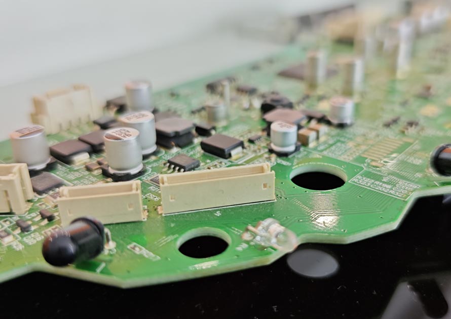
Flexible circuits are made of ultra-thin layers of Polyimide (PI) or PET, bonded with adhesives, and covered with thin copper traces. Because the substrate is mechanically unstable, it absorbs moisture, warps, and shifts dynamically during manufacturing.
When you separate FPCs, you face three massive risks on the production floor:
- Delamination: Mechanical pulling or tearing from blunt tools can separate the polyimide coverlay from the copper layers.
- Trace Fractures: Flex circuits are designed to bend after installation into the final product enclosure, not during the cutting process. A physical stamping tool can cause microscopic fractures in the traces near the board edge.
- Contamination: Physical cutting generates debris. If adhesive dust or copper swarf lands on a fine-pitch connector pad, the board will fail final electrical testing.
“Mechanical stress during depaneling is a hidden risk… it often leads to micro-cracks in solder joints and latent failures in ceramic capacitors (MLCCs).”— Source: Seprays Field Analysis
Method 1: Punching Depaneling (Die Cutting)
Punching relies on a custom-machined male/female die set—typically made of hardened tungsten steel—loaded into a mechanical or servo-driven press. It physically shears the FPC out of the panel in one single stroke.
The Benefits
- Unmatched Speed at Scale: Modern servo-controlled presses can operate at blistering speeds. For simple designs, a single punching machine can process tens of thousands of FPCs in a single shift.
- Lower Per-Unit Cost for Mass Production: According to industry research, for projects exceeding 1 million pieces annually, die-cutting costs can be over 40% lower than laser cutting.
- Clean Shearing (When Sharp): When the custom die is perfectly sharp, the cut is remarkably clean with minimal burrs.
The Drawbacks (The Hidden Costs)
- Massive Tooling Costs & Lead Times: Every single PCB design requires a custom steel die. If your layout engineer moves a component by 0.5mm, your expensive die is instantly rendered useless. Furthermore, fabricating these tools takes anywhere from 3 to 10 days, completely killing your agility for quick-turn prototyping.
- Tool Wear and Edge Tearing: Tungsten steel dulls. As the blade loses its edge, it stops cleanly shearing the polyimide and begins to stretch and tear it, causing edge delamination and latent defects.
When to Start Using Punching:
If you are an OEM locking in a design for a basic flexible LED strip and plan to manufacture millions of identical units over the next year without any design alterations, invest in a die-punching press immediately.
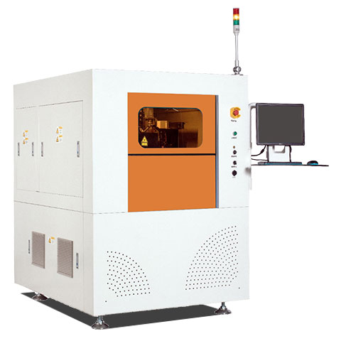
Method 2: Laser Depaneling (UV/Green Technology)
Laser technology separates FPCs through “cold ablation.” Instead of physically pushing a steel die through the material, the highly focused beam of light breaks the molecular bonds of the polyimide and copper, vaporizing the material layer by layer.
The Benefits
- True Zero Mechanical Stress: Because the laser beam never physically touches the board, there is absolutely no shearing force, stretching, or bending. The mechanical stress applied to the board remains virtually zero, completely eliminating the risk of cracked traces.
- No Tooling Costs or Delays: The “tool” is a software CAD file. You can cut Design A in the morning, load a new layout, and cut Design B in the afternoon. There are zero dies to buy, store, or send out for sharpening.
- No Carbonization on Polyimide: Modern UV lasers utilize ultra-short wavelengths (355nm) to minimize the Heat Affected Zone (HAZ). They cut through PI and PET cleanly without burning or carbonizing the edges, maintaining the board’s insulation resistance.
- Microscopic Kerf Width: A laser beam typically has a kerf (cut width) of only 20 to 50 micrometers (μm).
“Laser routing provides a significant advantage as the kerf width is only a few micrometers… compared to routing space which typically takes up 1.5 to 3 mm.”— Source: Circuitnet Depaneling Analysis
The Drawbacks
- Higher Upfront Investment: A high-quality UV laser system requires a larger initial capital expenditure than a basic mechanical punch press.
- Slower for Simple Shapes: If you are cutting out a basic large rectangle, a punch press does it instantly. A laser must physically trace the perimeter, which takes slightly longer per board for simple geometries.
When to Start Using Laser:
If you are an EMS provider handling high-mix orders (multiple different designs per week), or if you are manufacturing HDI flex circuits for medical wearables where any mechanical defect means a scrapped product, laser is your only viable path.
Best Practices: Optimizing FPC Yield on the Floor
Whether you lean toward punching or laser, how you integrate the machine dictates your success. Here are the best practices we implement when setting up automated pcb depaneling solutions for our clients.
Practice 1: Reclaim Panel Real Estate (Kerf Optimization)
If you switch to laser, you must update your panelization design rules. A physical punching die requires significant space between boards to prevent the steel web from breaking during the press stroke.
The Result: By nesting your FPC designs closer together (leveraging the 20μm laser kerf) and leaving as little as 0.2mm between boards instead of 2.0mm, you can fit 15% to 25% more circuits onto a single raw PI panel. This material savings alone often pays for the laser machine within the first year of operation.
“A 2D linear moving stage and UV laser… the laser beam diameter is only 20 μm after focusing.”— Source: De-panel Laser Specifications
Practice 2: Integrate Inline Automation with CCD Vision
Flexible circuits are notoriously difficult to handle by hand. Operators manually moving flimsy panels into a punch press often misalign them, resulting in a mis-cut that destroys the entire panel.
The Result: Feed your panels directly into an inline depaneling system. Using high-resolution CCD cameras to automatically align fiducial marks guarantees that the laser beam hits the exact right coordinates every single time, compensating for any material shrinkage and removing human handling errors entirely.
Practice 3: Counter-Pressure for Mechanical Processing
If your volume demands mean you must use a mechanical punch press, do not just slam the die into the unsupported material. Alternatively, if you are looking into v-cut depaneling alternatives for hybrid boards, you need structural support.
The Result: Implement strict counter-pressure settings (typically 0.1-0.3MPa) on the bottom die block. This holds the thin FPC perfectly flat during the shear cycle, drastically reducing the “elastic deformation” phase and minimizing burrs.
Data Breakdown: Punching vs. Laser Comparison
To help you present this business case to your engineering and procurement teams, here is a technical comparison of the two methods on the factory floor:
| Process Metric | Die Punching (Mechanical) | Laser Depaneling (UV/Green) |
| Component Stress | Moderate to High (Shearing force) | Zero (Non-contact process) |
| Edge Quality | Clean (when tool is sharp), tears when dull | Perfectly smooth, no carbonization |
| Tooling Cost | Extremely High (Custom dies for every design) | Zero (Software CAD driven) |
| Kerf Width Waste | High (Requires wide metal webs) | Microscopic (20μm to 50μm) |
| Setup Time | Slow (3-10 days for die fabrication) | Instant (CAD file upload) |
| Ideal Application | Locked designs, >1 Million volume, simple shapes | High-mix, complex HDI shapes, fragile components |
Conclusion: Why We Recommend Upgrading
Manufacturing flexible printed circuits is a game of micrometers and margins. Every board you scrap due to a torn polyimide edge, delamination, or a mechanically cracked trace destroys your factory’s profitability. If your facility runs massive volumes of unchanging designs, the raw speed of a custom punching die is a valid economic choice.
However, as the electronics industry pushes toward higher component density, tighter tolerances, and much faster product life cycles, the agility and absolute zero-stress guarantee of a laser cutting system make it the superior long-term investment. Stop letting outdated physical separation methods dictate your defect rate, and start protecting your yield with precision light ablation.
Frequently Asked Questions (FAQ)
1. Will a laser burn or carbonize the edges of my flexible PCB?
No, provided you use the correct laser source. Modern UV lasers (355nm) operate on a “cold ablation” principle with a very short wavelength. They vaporize the polyimide and PET materials so rapidly that the Heat Affected Zone (HAZ) is microscopic (often under 10 micrometers), resulting in extremely clean edges with no carbonization or electrical degradation.
2. How long does it take to get a new die made for punch depaneling?
Depending on the complexity of the flex circuit outline, fabricating a custom hardened tungsten steel die typically takes between 3 to 10 days. This lead time is a significant bottleneck if your R&D team is doing rapid prototyping or frequent design iterations.
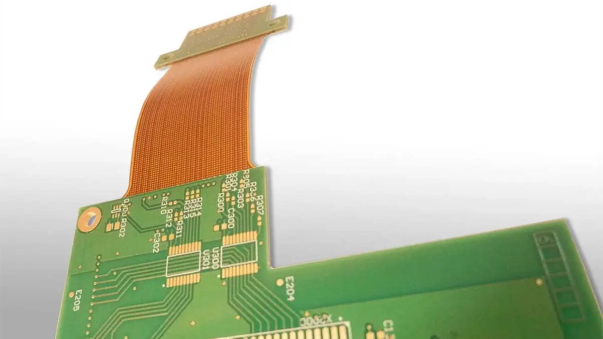
3. Which separation method is better for Rigid-Flex boards?
Laser depaneling is vastly superior for Rigid-Flex applications. Punching a board that has varying thicknesses (thick rigid FR4 sections intersecting with thin flex sections) requires highly complex, staggered dies that are expensive and prone to breaking. A laser automatically adjusts its focal depth, seamlessly cutting through both materials without stress.
4. Can I use a high-speed mechanical router to cut FPCs?
It is highly discouraged. A high-speed mechanical router bit will grab the flexible polyimide material, winding the thin fibers around the spinning bit. This causes severe edge tearing, trace delamination, and often destroys both the flexible circuit and the cutting tool.
5. Does laser depaneling actually save money on raw materials?
Yes, significantly. Because a UV laser beam has a kerf (cut width) of only 20 to 50 micrometers, layout engineers can nest FPC designs incredibly close together on the manufacturing panel. This kerf reduction minimizes wasted space and commonly increases the number of usable boards per panel by 15% to 25% compared to mechanical punching.