![]()
PCB punching process
Revolutionizing PCB Manufacture: The Ultimate Guide to PCB Punching and Depaneling
This article dives deep into the world of PCB punching and depaneling, exploring the latest technologies and methods used in modern printed circuit board (PCB) manufacturing. Whether you’re an electronics enthusiast, a seasoned engineer, or a procurement professional in a large electronics manufacturing company, understanding these processes is crucial. As the demand for smaller, more efficient electronic devices grows, the precision and efficiency of PCB manufacturing become paramount. This article will provide valuable insights into how leading companies like TP-LINK, Canon, BYD, and Foxconn leverage advanced PCB depaneling techniques to maintain their competitive edge. It’s worth reading because it not only explains the what and how but also the why behind the critical steps in PCB production, making it essential knowledge for anyone involved in the electronics industry.
1. What is PCB Depaneling and Why is it Crucial in Modern Electronics Manufacturing?
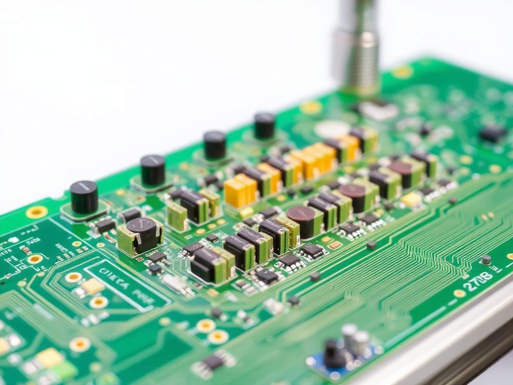
PCB depaneling is a critical step in the PCB manufacturing process where individual printed circuit boards (PCBs) are separated from a larger panel. This process is vital to ensuring the precision and quality of the final product. In the early stages of PCB fabrication, multiple PCBs are manufactured on a single panel to optimize material usage and streamline the production process. However, these individual PCBs must be separated before they can be used in electronic devices.
The importance of depaneling cannot be overstated. It directly impacts the functionality and reliability of electronic products. Poor depaneling can lead to mechanical stress, damage to circuit connections, and even short circuits. Leading electronics manufacturers like TP-LINK, Canon, and BYD invest heavily in advanced depaneling technologies to avoid these issues. For instance, our GAM 380AT PCB Bottom Depaneling Machine is designed to provide precise and stress-free separation, ensuring the integrity of each PCB. The use of the high quality machine in the PCB industry is vital. As a leading PCB depaneling machine manufacturer, we understand the specific requirements of different PCB types and provide customized solutions to meet these needs.
2. How Does the PCB Punching Process Work?
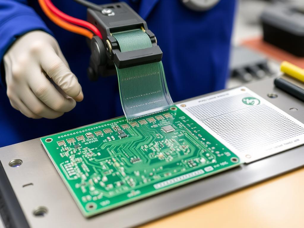
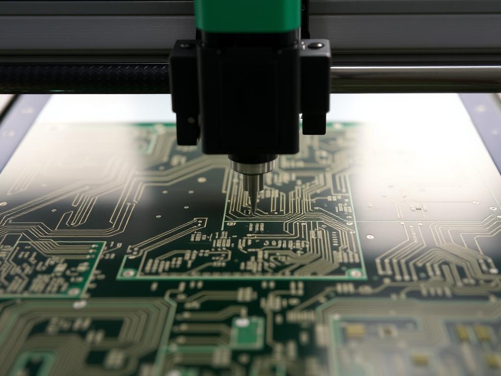
The PCB punching process is a traditional method used to separate individual printed circuit boards from a panel. This process involves the use of a specialized punching machine equipped with sharp blades on one part and supports on the other. The punching fixture holds the PCB in place while the punch is applied, effectively cutting through the substrate and separating the individual PCBs. It’s like using a precise cookie cutter for electronics. This step is crucial for smaller production runs or when dealing with PCBs that have irregular shapes.
Die punching is a common technique within the PCB punching process. It involves creating a custom die that matches the profile of the PCB. The die is then used to punch out the PCB from the panel. This method is particularly cost-effective for high-volume production as the initial investment in the die is offset by the speed and efficiency of the punching process. Our ZM10T & 15T PCB & FPC Punching Cutting Machine exemplifies how advanced machinery can streamline this process, offering precision and reliability for various PCB applications. The process uses the specialized punching fixture that consists of an upper and lower mold.
3. What Are the Different Types of Printed Circuit Board (PCB) Depaneling Methods?
There are several depaneling methods available, each with its own advantages and applications. The choice of method depends on factors such as the type of PCB, the size of the printed board, and the design requirements.
- V-Scoring: This method involves creating V-shaped grooves on the PCB panel using a specialized tool. The grooves weaken the substrate, allowing the individual PCBs to be easily broken apart. V-scoring is suitable for rigid PCBs and is commonly used in high-volume production.
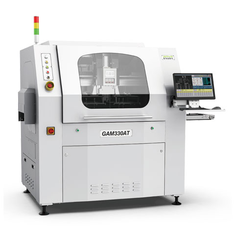
- Routing: PCB routing uses a router bit to cut the profile of the PCB, separating it from the panel. This method offers high precision and quality and is ideal for PCBs with complex shapes. Our GAM 330AT In-Line Automatic PCB Router Machine is a prime example of how routing can be automated for enhanced efficiency.
- Punching: As discussed earlier, punching uses a punching machine to cut through the substrate. It is cost-effective for high-volume production and suitable for various materials.
- Laser Depaneling: This advanced method uses a laser beam to cut the PCB, offering unparalleled precision and minimal mechanical stress. Laser depaneling is ideal for delicate PCBs and those requiring high accuracy.
4. How Does Laser Depaneling Revolutionize PCB Manufacturing?
Laser depaneling is a game-changer in the PCB manufacturing industry. Unlike traditional methods that involve physical contact with the PCB, laser depaneling uses a focused laser beam to cut through the substrate. This non-contact method eliminates mechanical stress, reducing the risk of damage to sensitive components and circuit connections.
One of the key advantages of laser depaneling is its precision. The laser beam can be controlled with extreme accuracy, allowing for intricate cuts and complex shapes. This makes it ideal for multilayer PCBs and flex circuits that require precise separation. Additionally, laser depaneling produces clean edges, reducing the need for post-processing steps. Our DirectLaser H3 Laser Online Machine harnesses the power of laser technology to deliver superior depaneling solutions for a wide range of PCB applications.
5. What Role Does Automation Play in PCB Depaneling and Punching?
Automation is transforming the PCB manufacturing process, and depaneling is no exception. Automated depaneling machines offer significant advantages over manual methods, including increased speed, improved precision, and reduced labor costs. These machines can handle large volumes of PCBs quickly and efficiently, making them ideal for mass production.
Automated punching machines, such as our ZM10TS / 15TS PCB & FPC Punching Cutting Machine, are equipped with advanced features that enhance the punching process. These features include automatic optical inspection systems that ensure accurate alignment and cutting, as well as programmable controls that allow for customization based on the specific requirements of the PCB. By automating the depaneling and punching processes, manufacturers can achieve higher throughput, consistent quality, and reduced operational costs.
6. How Can V-Groove Depaneling Enhance PCB Production Efficiency?
V-Groove depaneling is a widely used method for separating individual PCBs from a panel. This technique involves creating V-shaped grooves on the PCB panel using a specialized tool. The grooves weaken the substrate, making it easy to break apart the individual PCBs along the scored lines.
One of the main advantages of V-Groove depaneling is its simplicity and cost-effectiveness. It does not require complex machinery or expensive tools, making it accessible to a wide range of PCB manufacturers. Additionally, V-Groove depaneling is suitable for rigid PCBs and can be used for both single-sided and double-sided PCBs. Our ZM30-ASV Fully Automatic saw-type V-groove PCB depaneling machine is designed to optimize this process, providing efficient and reliable depaneling for high-volume production.
7. What Are the Key Considerations for Choosing a PCB Depaneling Machine?
Choosing the right PCB depaneling machine is crucial for ensuring the efficiency and quality of your PCB manufacturing process. Several factors should be considered when making this decision:
- Type of PCB: Different depaneling methods are suitable for different types of PCBs. For example, laser depaneling is ideal for delicate or complex PCBs, while V-Groove depaneling is suitable for rigid PCBs.
- Production Volume: The volume of PCBs you need to process will influence the type of machine you choose. Automated machines are ideal for high-volume production, while manual methods may suffice for smaller runs.
- Precision Requirements: The level of precision required for your PCBs will also impact your choice. Laser depaneling offers the highest precision, while punching and routing provide good precision for most applications.
- Budget: The cost of the depaneling machine is another important consideration. While advanced machines like our DirectLaser H1 High-Precision Laser Cutting Machine offer superior performance, they come with a higher price tag. It’s essential to balance performance with cost to find the best solution for your needs.
8. How Do Leading Companies Optimize Their PCB Manufacturing Process?
Leading electronics manufacturers like TP-LINK, Canon, BYD, Flex, TCL, Xiaomi, Lenovo, OPPO, HONOR, and Foxconn optimize their PCB manufacturing process by investing in advanced technologies and automation. These companies understand that the quality of their products depends on the precision and efficiency of each step in the manufacturing process, including depaneling.
For example, these companies often use our SMT In-Line Depaneling Machine Solution to integrate depaneling seamlessly into their production lines. This not only speeds up the process but also ensures consistency and reduces the risk of errors. Additionally, they leverage data analytics and real-time monitoring to identify bottlenecks and optimize their operations continuously.
9. What Are the Future Trends in PCB Depaneling Technology?
The PCB manufacturing industry is constantly evolving, and depaneling technology is no exception. Several trends are shaping the future of PCB depaneling:
- Increased Automation: Automation will continue to play a crucial role in PCB depaneling, with more advanced machines capable of handling complex tasks with minimal human intervention.
- Integration with AI and Machine Learning: Artificial intelligence (AI) and machine learning will be integrated into depaneling machines to improve precision, optimize processes, and predict maintenance needs.
- Miniaturization: As electronic devices become smaller, the demand for smaller PCBs will increase. This will drive the development of depaneling technologies capable of handling micro-PCBs with extreme precision.
- Sustainability: Environmental concerns will push manufacturers to adopt more sustainable depaneling methods. This includes reducing material waste, minimizing energy consumption, and using eco-friendly materials.
10. How Can Your Business Benefit from Advanced PCB Depaneling Solutions?
Investing in advanced PCB depaneling solutions can bring numerous benefits to your business:
- Improved Product Quality: Advanced depaneling methods like laser depaneling ensure precision and minimize the risk of damage to PCBs, resulting in higher quality products.
- Increased Efficiency: Automated depaneling machines can process large volumes of PCBs quickly and efficiently, reducing production time and labor costs.
- Cost Savings: By optimizing the depaneling process and reducing errors, you can minimize material waste and rework, leading to significant cost savings.
- Competitive Edge: Using state-of-the-art depaneling technology can give your business a competitive edge by enabling you to produce high-quality PCBs faster and more efficiently than your competitors.
FAQs
- What is the difference between single-sided and double-sided PCBs? Single-sided PCBs have a conductive layer on only one side of the substrate, while double-sided PCBs have conductive layers on both sides. Double-sided PCBs allow for more complex circuit designs and higher component density. This type of PCB is widely used.
- How does the etching process work in PCB fabrication? The etching process involves removing unwanted copper foil from the PCB to create the desired circuit pattern. This is typically done by applying a photoresist layer to the PCB, exposed to ultraviolet light through a mask, and then using a chemical solution to dissolve the exposed copper.
- What is solder mask and why is it important? Solder mask is a protective layer applied to the PCB to prevent solder from bridging between conductive areas and causing short circuits. It also protects the copper traces from corrosion and mechanical damage.
- What are Gerber files and how are they used in PCB manufacturing? Gerber files are standard file formats used in the PCB manufacturing industry to describe the printed circuit board images: copper layers, solder mask, legend, drill data, etc. These files are used by PCB manufacturers to fabricate the PCB according to the design requirements.
- What is lamination in multilayer PCB fabrication? Lamination is the process of bonding together different layers of the PCB using heat and pressure. In multilayer PCB fabrication, multiple inner layer cores are stacked with prepreg (epoxy resin impregnated glass fabric) and copper foil, and then laminated to create a single, solid PCB.
- How can I get a quote for PCB depaneling machines? You can contact us through our website to request a quote for our PCB depaneling machines. Our team will be happy to provide you with detailed information and pricing based on your specific requirements.
Conclusion
In summary, PCB depaneling is a critical step in the PCB manufacturing process that directly impacts the quality and reliability of electronic products. Understanding the different depaneling methods, such as V-scoring, routing, punching, and laser depaneling, is essential for optimizing your PCB production. Investing in advanced depaneling solutions, such as our PCB router machines and laser machines, can bring numerous benefits to your business, including improved product quality, increased efficiency, cost savings, and a competitive edge.
- PCB depaneling is a crucial step in manufacturing.
- Multiple methods exist, each with unique advantages.
- Automation and advanced technologies enhance efficiency.
- Leading companies optimize processes with cutting-edge solutions.
- Future trends include increased automation and AI integration.
- Investing in advanced depaneling solutions improves quality and competitiveness.
- The PCB is the basic element in the modern electronics circuit boards.
By staying informed about the latest developments in PCB depaneling technology and partnering with a trusted manufacturer like us, you can ensure that your business stays ahead of the curve in the rapidly evolving electronics industry. Contact us today to learn more about how our PCB depaneling solutions can benefit your business.
