![]()

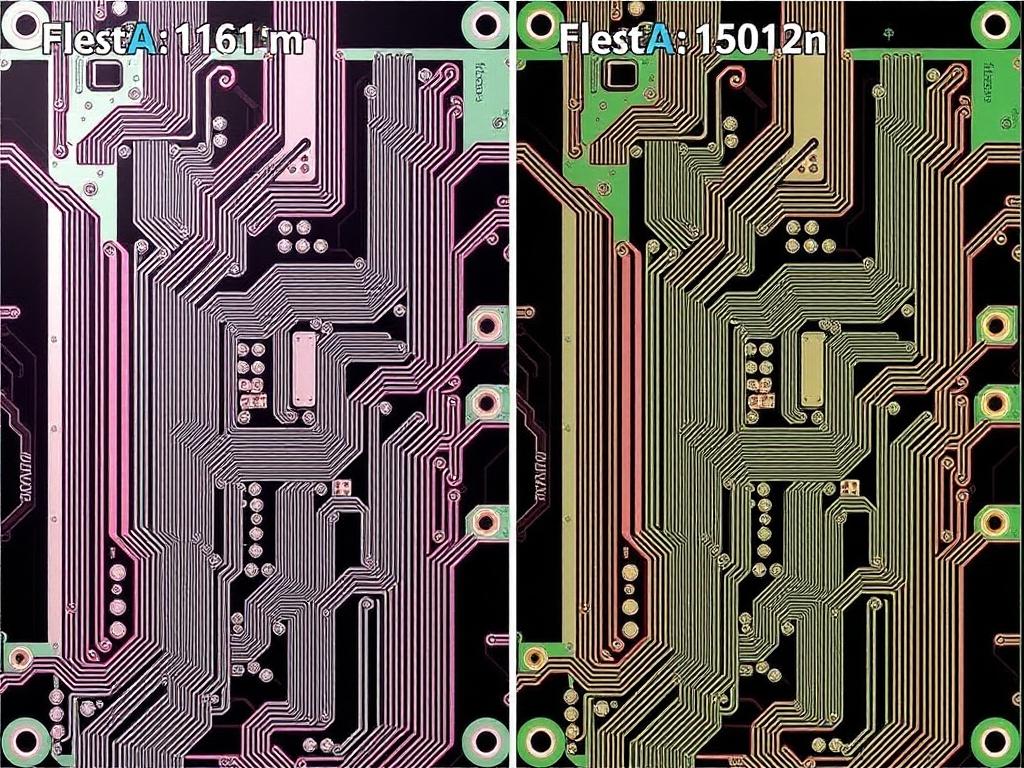
PCB depaneling speed comparison
Precision PCB Depaneling: Moving from Manual Methods to Laser Excellence
For over two decades, I’ve witnessed the evolution of PCB depaneling firsthand. What was once a painstaking manual process is now a realm of sophisticated technology, with laser depaneling leading the charge. This article delves into the fascinating world of pcb depaneling, exploring various methods of pcb depaneling, and highlighting why transitioning from manual to laser solutions is not just an upgrade, but a strategic imperative for modern electronics manufacturing. If you’re involved in cutting pcbs or struggling with the challenges of pcb separation, this guide offers valuable insights into optimizing your depaneling process.
PCB Depaneling: Why Is It Necessary and What Are the Traditional Depaneling Methods?
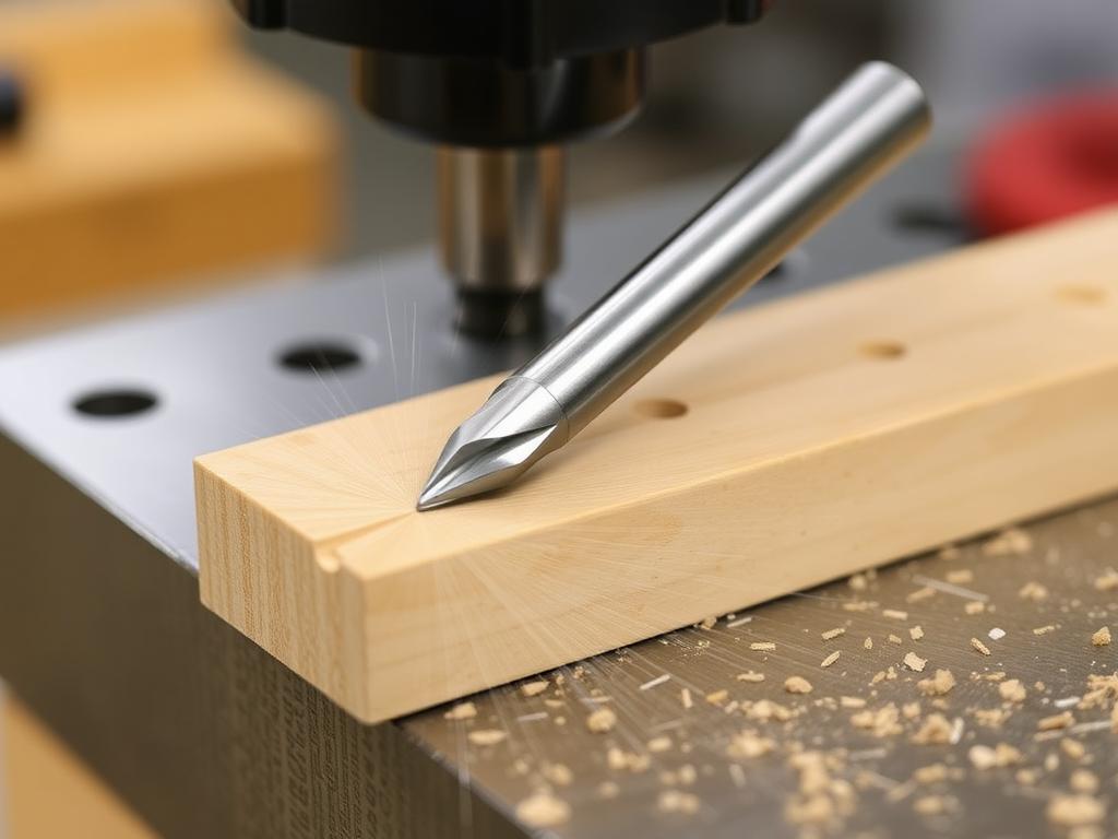
As someone deeply entrenched in the pcb manufacturing landscape, I can tell you that depaneling is a crucial step. Imagine a large sheet of interconnected pcbs, like a meticulously crafted puzzle. This is how pcbs are often manufactured for efficiency – a process called panelization. Depaneling is simply the act of separateing these individual pcbs into their final, functional forms. Over the years, I’ve seen various depaneling methods come and go. Traditional approaches often involved manual breaking along v-scoring, or employing mechanical methods like routers and mills. While these separation methods served their purpose, they often introduced mechanical stress to the delicate circuit board, risking damage and impacting the overall quality.
Think of it like this: trying to neatly tear apart a sheet of stamps versus using precise scissors. The former introduces stress and potential tears, while the latter offers a clean cut quality. Traditional methods, especially for intricate pcb designs or thin substrate materials, could lead to issues like burrs, dust contamination, and even component damage due to the physical force applied during the cutting process. For manufacturers like TP-LINK and Canon, where precision is paramount, these limitations are significant.
What Makes Laser Depaneling a Game Changer in PCB Separation?
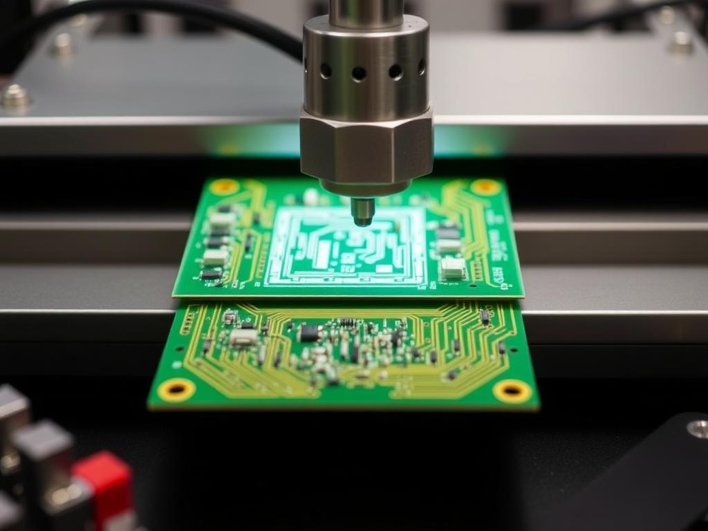
In my experience, the arrival of laser depaneling marked a true revolution. Unlike traditional mechanical methods, laser cutting is a non-contact process. A highly focused laser beam precisely separates the pcbs by ablation, essentially vaporizing the panel material layer by layer. This eliminates the mechanical stress associated with sawing or routing, leading to significantly improved cut quality and reduced risk of damage.
Consider the intricate designs of modern electronics, especially for companies like BYD and Flex. The ability of laser depaneling to handle complex contours and tight spaces without inducing stress is a major advantage. We’re talking about clean edges, minimal debris, and a higher yield rate – all contributing to greater cost-effectiveness in the long run. From my perspective, witnessing this shift has been remarkable. We’ve gone from concerns about micro-fractures to the near-perfect singulation offered by laser technology.
How Does Laser Technology Work in PCB Depaneling?
The magic behind laser depaneling lies in the precise control of the laser beam. Different types of laser sources can be used, but for pcb applications, uv lasers are particularly effective. The shorter uv wavelengths allow for finer control and cleaner ablation, minimizing the heat-affected zone and further reducing the risk of damage to sensitive components or the solder. The laser power, cutting speed, and focused spot size are carefully calibrated based on the material thickness and type of pcb.
Imagine the laser beam as an incredibly precise and tiny cutting tool, moving along the predefined path with unmatched accuracy. This precision allows for intricate cuts and the ability to separate even densely populated printed circuit boards without impacting nearby components. For high-volume manufacturers like TCL and Xiaomi, the speed and precision of laser depaneling translate directly into increased throughput and efficiency in their manufacturing process.
What Are the Key Advantages of Laser-Based PCB Depaneling?
Having seen countless depaneling operations, I can confidently say that laser-based pcb depaneling offers significant advantages. The elimination of mechanical stress is paramount, especially for flexible pcbs (FPCs) or those with delicate components. The superior cut quality, with smooth edges and minimal burrs, reduces the need for secondary cleaning processes, further enhancing cost-effectiveness.
Here’s a quick rundown of the benefits:
- High Precision: Capable of intricate cuts and complex shapes.
- Minimal Stress: Protects delicate components and reduces micro-fractures.
- Cleanliness: Reduces dust and debris contamination.
- Flexibility: Suitable for various pcb materials and thicknesses.
- Speed: Offers faster cutting speed compared to mechanical methods, improving throughput.
- Reduced Tooling Costs: No physical blades or bits to wear down or replace.
- Automation: Easily integrated into automated production lines.
For companies like Lenovo and OPPO, striving for high-quality products, the precision and reliability of laser depaneling are invaluable.
What Types of PCBs Benefit Most from Laser Depaneling?
While laser depaneling offers benefits across the board, certain types of pcbs particularly shine with this technology. Flexible pcbs, due to their delicate nature, are ideal candidates. The non-contact nature of laser cutting prevents the damage that mechanical methods might inflict. High-density interconnect (HDI) pcbs, with their closely packed components, also benefit from the precision of laser depaneling, minimizing the risk of collateral damage.
Furthermore, pcbs with complex shapes or internal cutouts that are difficult to achieve with traditional methods are perfectly suited for laser ablation. Even standard rigid printed circuit boards benefit from the clean edges and reduced stress offered by laser depaneling. Think of the intricate designs in HONOR and Foxconn products – laser depaneling enables their precise creation and separation.
Manual to Laser: Is the Transition Worth It for PCB Manufacturing?
From my perspective, having witnessed the evolution firsthand, the transition from manual to laser depaneling is not just worthwhile, it’s becoming increasingly necessary for staying competitive. While the initial investment in laser systems might seem higher, the long-term cost-effectiveness outweighs the initial outlay. Reduced material waste, lower reject rates due to improved cut quality, and decreased labor costs associated with manual separation methods all contribute to a significant return on investment.
Moreover, the increased precision and ability to handle complex pcb designs open up new possibilities for product innovation. For smaller pcb players as well as large panels containing multiple boards, adopting laser depaneling can be a game-changer in terms of efficiency and product quality. It’s about investing in the future of your manufacturing process.
Addressing the Challenges of PCB Cutting with Laser Technology
While laser depaneling offers numerous advantages, it’s important to acknowledge potential challenges. For thicker pcbs, multiple passes of the laser beam might be required, potentially impacting cutting speed. Choosing the right laser source, particularly the uv laser, and optimizing parameters like laser power and cutting speed are crucial for achieving optimal results.
Furthermore, the kerf width, the amount of material removed by the laser, needs to be considered during the pcb design phase. Proper ventilation and fume extraction are also essential for a safe working environment. However, advancements in laser technology and depaneling systems are continuously addressing these challenges, making laser depaneling an increasingly robust and reliable solution.
Why Choose Us for Your PCB Depaneling Needs?
With 20 years in this industry, I’ve seen what works and what doesn’t. At pcbdepaneling.com, we offer a comprehensive range of depaneling solutions, including state-of-the-art pcb router machines, precise pcb laser depaneling systems, efficient v-groove depaneling machines, and robust pcb/fpc punching machines. We also provide essential accessories and solutions for the smt whole line equipment. Our automatic equipment is designed to seamlessly integrate into your production line, optimizing your entire depaneling process.
Our commitment is to provide solutions tailored to your specific needs. Whether you’re a small startup or a Fortune 500 giant like the esteemed companies we serve – TP-LINK, Canon, BYD, Flex, TCL, Xiaomi, Lenovo, OPPO, HONOR, and Foxconn – we have the expertise and the technology to elevate your pcb separateion process. We understand the nuances of panelization and can help you choose the most effective depaneling technique for your specific application.
Ready to Optimize Your PCB Depaneling Process?
The future of pcb manufacturing lies in precision and efficiency. Laser depaneling offers a pathway to achieve both. If you’re looking to move from manual to laser, improve your cut quality, reduce mechanical stress, or simply streamline your depaneling process, we’re here to help.
Ready to take the next step? Explore our range of PCB Router Machines, including the high-performance GAM 380AT PCB Bottom Depaneling Machine. For advanced laser depaneling solutions, consider our cutting-edge DirectLaser H5 PCB-FPC Laser Cutting Machine. If v-scoring is your preferred method, our ZM30-P PCB Guillotine Separator offers reliable performance. And for those needing automated solutions, our GAM 630V Automatic Sorting and Palletizing Machine can significantly boost your throughput. We also offer essential Milling Cutter accessories to keep your operations running smoothly. Discover our comprehensive SMT In-Line Depaneling Machine Solution for seamless integration.
Contact us today to discuss your specific needs and discover how our expertise and cutting-edge technology can transform your PCB depaneling process.
FAQs About PCB Depaneling
What are the main methods of PCB depaneling? Several methods exist, including manual breaking along v-scoring, mechanical routing or milling, punch pressing, and laser depaneling. The best depaneling method depends on the pcb design, material, volume, and required precision.
Is laser depaneling suitable for all types of PCBs? While highly versatile, laser depaneling is particularly advantageous for flexible pcbs, HDI pcbs, and boards with intricate shapes. Material thickness and the presence of sensitive components are also factors to consider.
How does laser depaneling compare to mechanical routing in terms of stress on the PCB? Laser depaneling is a non-contact process, eliminating the mechanical stress associated with routers and mills. This is a significant advantage for delicate circuit boards.
What are the cost considerations for implementing laser depaneling? While the initial investment in laser systems might be higher, the long-term cost-effectiveness is often greater due to reduced material waste, lower reject rates, and decreased labor costs. The absence of cutting tools also reduces operational expenses.
What safety measures are required for laser depaneling? Proper ventilation and fume extraction are essential to remove any byproducts generated during the laser ablation process. Laser safety training for operators is also crucial.
Key Takeaways:
- PCB depaneling is a critical step in electronics manufacturing.
- Laser depaneling offers significant advantages over traditional methods, including higher precision and reduced stress.
- UV lasers are particularly effective for pcb separateion due to their shorter wavelengths.
- The transition from manual to laser depaneling can lead to greater cost-effectiveness and improved product quality.
- Choosing the right depaneling method depends on your specific needs and pcb characteristics.