![]()

PCB depaneling for medical devices
PCB Depaneling: From Manual to Laser – A 20-Year Journey Through Methods of PCB Depaneling
As someone who’s spent the last two decades immersed in the world of pcb manufacturing, I’ve seen firsthand the evolution of depaneling methods. From the days of manual separation to the precision of laser depaneling, the way we separate individual pcbs from larger panels has drastically changed. This article will explore these changes, focusing on different methods of pcb depaneling including the rise of laser technology. This is more than just a technical overview; it’s a practical look at the solutions that keep our electronics industry moving forward. If you’re involved in pcb manufacturing, especially if you’re a player in the electronics industry, this deep dive into pcb depaneling is designed to give you the inside knowledge you need.
What is PCB Depaneling and Why is it Necessary?
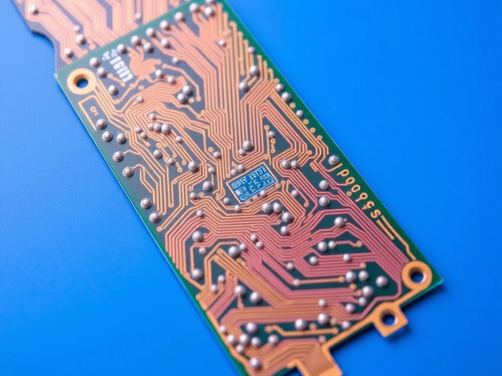
In the manufacturing process of flexible printed circuit boards, or any printed circuit board for that matter, pcbs are typically produced in large panels, each containing multiple boards. This approach, called panelization, is efficient for mass production. However, these individual pcbs need to be separated or ‘broken out’ into individual printed circuit boards for use in electronic devices. This is where depaneling comes in. The depaneling process is the method of removing individual circuit boards from the larger panel. It’s not just a simple act of separation; the method used can significantly impact the integrity and quality of each separated pcb. This entire process of removing individual boards is also called singulation.
The importance of depaneling cannot be overstated. A poorly executed process can introduce mechanical stress, which can damage delicate components, components and traces, and solder joints, especially those close to the edge of the circuit. For high-density pcbs, where accuracy is critical, selecting the correct depaneling method is crucial. The entire circuit board relies on a precise and clean separation. It’s not enough just to separate the boards; we need to ensure the manufacturing process is as gentle as possible. This is a fundamental step in ensuring the final products are reliable and functional.
What are the Traditional Methods of PCB Depaneling?
Before the advent of advanced technologies like laser cutting, several methods were used to separate pcbs. One common approach was manual depaneling, where a tool is used to create a score line along the panel and then the individual circuit boards are physically snapped apart. This method is cost-effective for small-scale production but introduces significant mechanical stress and can lead to inconsistencies. Another traditional method involved using a saw or a router. With routing, a tool is used to cut along the pre-designed cut line. Router cutting can be more accurate than manual methods but still introduces stress and is not ideal for densely populated or flexible boards.
These methods, while still in use, present several limitations. Manual depaneling relies heavily on operator skill and consistency, leading to varying quality. The use of a tool like a saw or router can cause significant part induced stress and generate dust, requiring additional cleaning. Additionally, the cutting process also creates a cut kerf, which is the width of the material removed during cutting. This kerf width affects the overall dimensions of the individual pcbs, and when using mechanical methods, we often see a larger, less controlled cut kerf. In the early days, these challenges were just a part of the manufacturing process, but we’ve come a long way since then.
What are the Key Challenges of Traditional Depaneling Methods?
Traditional depaneling methods, while functional, have several inherent challenges. One of the most significant issues is the mechanical stress they introduce to the pcb. Manual snapping, sawing, or even router cutting applies considerable force to the board, which can damage sensitive surface mount technology (SMT) components, as well as thin flex circuits. This is particularly concerning for high-density pcbs or pcbs made of more fragile materials. The risk of cracking, delamination, and bending is always present, especially when dealing with smaller pcbs.
Another challenge is the lack of precision. Manual methods lack the accuracy needed for today’s complex designs, and even mechanical methods like router cutting are limited by the tool size and its movement. These limitations can lead to inconsistent kerf width, which can affect the final dimensions and fit of the individual pcbs within electronic devices. The physical contact of the tool in traditional methods also introduces dust and debris, increasing the need for secondary cleaning process of flexible printed circuit. Finally, throughput, the rate at which boards can be separated, is also slower compared to modern methods, making these traditional approaches less suitable for large quantities of pcbs. These challenges drove the need for more precise and less damaging depaneling methods.
How Has Laser Technology Revolutionized PCB Depaneling?
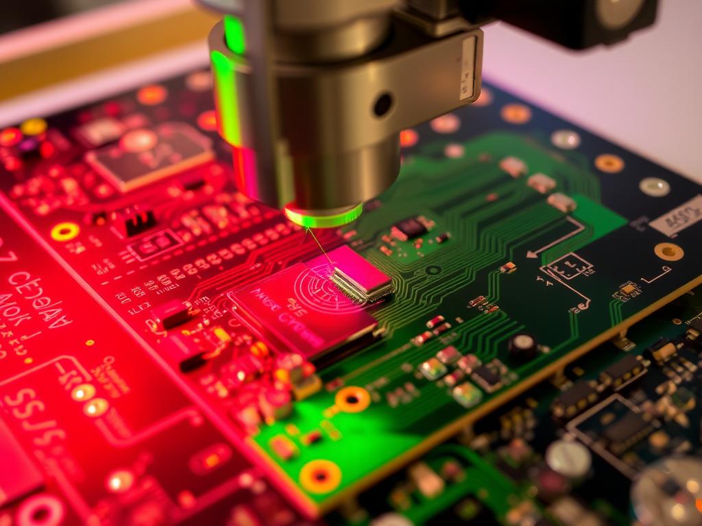
The introduction of laser technology has completely changed the landscape of pcb depaneling. Laser depaneling offers a non-contact approach to separating individual printed circuit boards from the panel. Instead of relying on physical tools, a focused laser beam precisely cuts through the pcb material, eliminating the mechanical stress associated with traditional methods. This method is particularly useful for delicate or complex pcbs where physical methods could cause damage. The transition from manual to laser was a giant leap, greatly increasing the accuracy and precision of depaneling.
Laser systems offer incredible flexibility and are adaptable to a wide variety of pcb materials, including fr4, polyimide, and other composites commonly used in today’s devices. The computer controlled process also allows for highly accurate cuts, reducing the cut kerf width and enabling the creation of intricately shaped individual pcbs. This laser cutting method can cut both rigid pcbs as well as flex pcb. Moreover, laser cutting is extremely precise, minimizing dust and debris, which is an important factor for maintaining the cleanliness of the circuit board. The ability to perform laser depaneling without physical contact has been revolutionary for the pcb manufacturing industry.
What are the Advantages of Using Laser for PCB Depaneling?
The advantages of using laser for pcb depaneling are numerous. Primarily, laser technology provides a non-contact method, eliminating any risk of mechanical stress and subsequent damage. This is especially crucial for handling sensitive, high-density, and thin and flexible circuit boards, including flex pcb and rigid flex pcbs, which are increasingly common in electronic devices like including smartphones, wearables, and medical technology. Laser depaneling also offers significantly higher levels of precision than traditional methods. The focused spot size of a laser beam allows for extremely fine cuts, accommodating even the most complex board shapes.
Moreover, the laser method drastically reduces debris and dust, resulting in a cleaner and more efficient depaneling process. This non-contact method allows for a much narrower kerf width which is a significant advantage. The computer-controlled nature of laser depaneling systems provides consistent, repeatable results, ensuring that every individual pcb is separated accurately and reliably. With laser cutting, there is also the advantage of speed, cutting speed is a key benefit. Overall, the use of laser in depaneling provides exceptional accuracy, minimizes damage, and speeds up the overall manufacturing process. This efficiency is why many pcb manufacturers have adopted the laser depaneling systems.
What is the Difference Between Router Cutting and Laser Cutting?
While both router cutting and laser cutting are methods of pcb depaneling, they operate on fundamentally different principles. Router cutting is a mechanical process, where a rotating cutting tool is used to cut along the cut line. This physical contact can introduce mechanical stress and may lead to inconsistent cuts. The kerf width is determined by the diameter of the tool, which limits the precision achievable. In contrast, laser cutting is a non-contact method that uses a focused laser beam to vaporize the pcb material.
Laser cutting has several advantages over router cutting. First, as we discussed, it is a non-contact method, eliminating mechanical stress and its potential for damage. Second, laser cutting offers much higher precision due to the small focused spot size of the laser beam. Also, the kerf width in laser cutting is much narrower and more consistent than with router cutting. Additionally, laser cutting creates minimal dust and debris, while router cutting can produce a considerable amount. While router cutting may be suitable for certain less delicate applications, laser cutting is the preferred choice for high-precision, sensitive, and complex pcbs. Finally, compared to router cutting, laser technology provides simultaneous cutting.
What are the Key Considerations When Choosing a Depaneling Method?
Selecting the appropriate depaneling method involves a number of critical considerations. The complexity and sensitivity of the pcb itself is often paramount. For simple, robust boards, traditional methods like routing might still be sufficient, however, for dense, thin, and flexible boards, laser depaneling is generally the safer and better choice. The volume of production is another significant factor. Laser depaneling systems are suitable for both small and large quantities, while other methods might have limitations when the throughput and the need for consistency are a priority. Additionally, we must think about pcb materials and the materials that they are made from.
The level of precision required for the pcb is another important consideration. High-precision boards with intricate designs benefit from the exactness of laser cutting, while less complex designs can sometimes be separated with mechanical methods. The budget is also a major consideration. Initial investment costs of laser systems may be higher, but the long-term benefits in terms of reduced damage, increased speed, and higher quality can be significant, reducing the need for rework. It’s essential to weigh all these factors carefully when making the decision and selecting a specific depaneling approach.
How is Flex PCB Depaneling Different from Rigid PCB Depaneling?
Flex pcb depaneling plays a crucial role in modern electronics, and it presents some unique challenges compared to rigid pcb depaneling. The nature of flex pcb materials, which are typically made of polyimide or similar thin and flexible circuit boards, makes them far more susceptible to damage from mechanical stress. Traditional depaneling methods like snapping, sawing or even routing are unsuitable for most flex applications. In these cases, methods of pcb depaneling involving direct contact of the tool are more likely to cause tearing, delamination, and damage.
Laser depaneling is the preferred method for flex pcb, due to its non-contact nature and high precision. The laser beam can cut through the flex material without applying pressure, minimizing the risk of damage. The narrower kerf width offered by laser cutting also allows for more intricate designs and tighter spacing between individual pcbs. The speed and accuracy of the laser also help to maintain the integrity of the delicate components. Choosing the right depaneling method is therefore crucial when working with flex pcbs, as they are very susceptible to damage during the process, which is why the laser technology is highly favored.
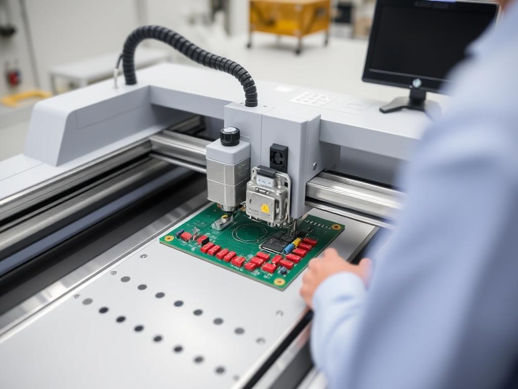
What Role does Automation Play in Modern Depaneling Systems?
Automation is playing an increasingly important role in modern depaneling systems. Automatic depaneling systems increase throughput and reduce human error. We automate various processes, such as loading the panels, executing the cut line, and unloading the finished boards, which reduces the need for manual handling and greatly increases efficiency. The integration of robotics, computer vision, and sophisticated control systems has greatly improved both precision and speed of the depaneling process.
Laser depaneling systems are particularly suitable for automation. Many include automated loading, laser beam adjustment, and automated unloading systems. Advanced laser depaneling systems even have automated vision systems that can scan the pcb and adjust the cut path in real-time, which further enhances precision. Automation allows for seamless integration into an SMT line as well. In summary, automation significantly enhances depaneling systems, which not only maximizes throughput and precision but also improves overall efficiency of the entire pcb manufacturing process.
What Does the Future of PCB Depaneling Look Like?
The future of pcb depaneling will likely be dominated by advancements in laser technology and further integration of automation. We expect to see more efficient, higher-speed laser systems with improved beam shaping and control. These improvements will allow for even more precise cuts, narrower cut kerf width, and increased cutting speed. The use of uv laser is also expected to grow, as it can cut different materials more effectively and accurately. We expect to see much more flexibility regarding various pcb materials.
Furthermore, we anticipate a further blurring of lines between depaneling and other manufacturing processes. With smarter software and more interconnected systems, depaneling will become an integral part of a fully automated manufacturing process. Automation and robotics will make the depaneling process even more efficient. We anticipate more intelligent systems that can adapt to different pcb designs and materials in real-time. In short, the future of pcb depaneling is one of increased precision, speed, automation, and greater flexibility to meet the evolving needs of the electronics industry.
Frequently Asked Questions
What is the difference between depaneling and singulation?
Depaneling and singulation are two terms that are often used interchangeably. Both refer to the process of separating individual pcbs from a larger panel. It is also called singulation.
Why is laser depaneling considered a superior method?
Laser depaneling is considered superior because it is a non-contact method. It provides the best precision, reduces mechanical stress, and minimizes dust and debris. The precision and the non-contact method both make it ideal for use with the most sensitive, high-density, and complex pcbs.
Can all PCB materials be depanelled with a laser?
Laser depaneling is compatible with a wide variety of pcb materials, including FR4, polyimide, and other composite materials used in pcb manufacturing. However, the specific laser source and parameters might need to be adjusted based on the properties of the material.
What is the benefit of automation in the depaneling process?
Automation in the depaneling process helps to increase throughput, reduce human error, and improve overall efficiency and consistency. It also ensures that every individual printed board is handled accurately and reduces the risk of damage.
What type of companies use depaneling machines?
Our depaneling machines are used by a wide range of companies in the electronics industry, including electronic technology companies, large electronic product processing factories, and individual pcb players. Our products are trusted by industry giants like TP-LINK, Canon, BYD, Flex, TCL, Xiaomi, Lenovo, OPPO, HONOR, and Foxconn.
Key Takeaways
- PCB depaneling is the process of separating individual pcbs from a larger panel.
- Traditional depaneling methods such as manual separation and router cutting, involve mechanical stress, which can damage delicate components and traces.
- Laser depaneling is a non-contact method that provides high precision, reduces mechanical stress, and minimizes dust and debris.
- The choice of depaneling method depends on the complexity and sensitivity of the pcb, production volume, and budget.
- Flex pcb depaneling requires a high precision method used due to the sensitivity of the materials used. Laser is the preferred choice.
- Automation is playing an increasingly important role in modern depaneling systems, increasing the precision and the speed.
- The future of depaneling will be shaped by further improvements in laser technology and more automation, reducing labor costs.
This in-depth look at pcb depaneling should provide a wealth of information for everyone in the pcb manufacturing industry. If you’re looking to upgrade your manufacturing process or exploring the best options for your pcb production, please get in touch. As a leading PCB depaneling machine manufacturer, we offer a range of solutions tailored to your specific requirements, just like the solutions we provide for TP-LINK, Canon, BYD, Flex, TCL, Xiaomi, Lenovo, OPPO, HONOR, Foxconn and many other leading tech brands. Discover our range of high-precision PCB router machines for separating your panels efficiently and accurately, or, for more sensitive applications, explore the precision of our laser depaneling solutions for an even greater precision. Don’t forget to check out our V-Groove Depaneling options for reliable, cost-effective solutions, or consider our robust PCB/FPC Punching Machine when high-volume throughput is key. And for a fully optimized production line, take a look at our advanced Automatic Equipment. Don’t forget that we also offer essential Accessories to keep your operations smooth.
Contact us today to learn more about how we can help you optimize your pcb manufacturing process.
Learn more about our PCB Router Machines Explore our range of V-Groove Depaneling Solutions Discover the precision of our PCB Laser Depaneling options Learn more about our PCB/FPC Punching Machines Explore our Automatic Equipment solutions Check out our range of accessories