![]()

PCB depaneling for high-volume production
Streamlining Your PCB Separation: Mastering PCB Depaneling Methods for Printed Circuit Boards
For over two decades, I’ve been at the forefront of pcb depaneling, witnessing firsthand the evolution of this crucial step in electronics manufacturing. From the basic hand-separation methods to the sophisticated automated systems of today, the journey has been marked by continuous innovation. This article dives deep into the world of depaneling, exploring the various methods available for printed circuit board separation. Understanding these techniques – from the precision of routers to the speed of punch methods – is essential for anyone involved in printed circuit production, whether you’re a burgeoning startup or a large-scale manufacturer. Let’s unlock the secrets to efficient and effective pcb separation.
A Comprehensive Look at PCB Depaneling: Methods and Best Practices
What exactly is depaneling, and why does it matter so much in the creation of printed circuit boards? Let’s explore the core concepts and various approaches to this essential process.
What is Depaneling and Why is it a Critical Step for PCBs?
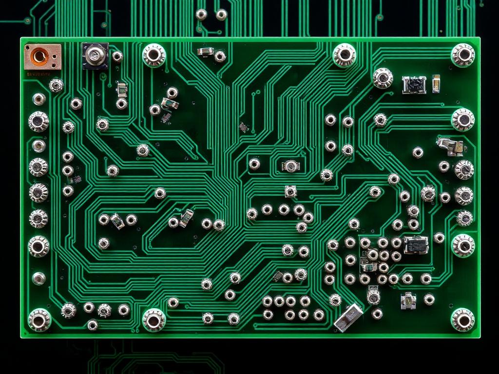
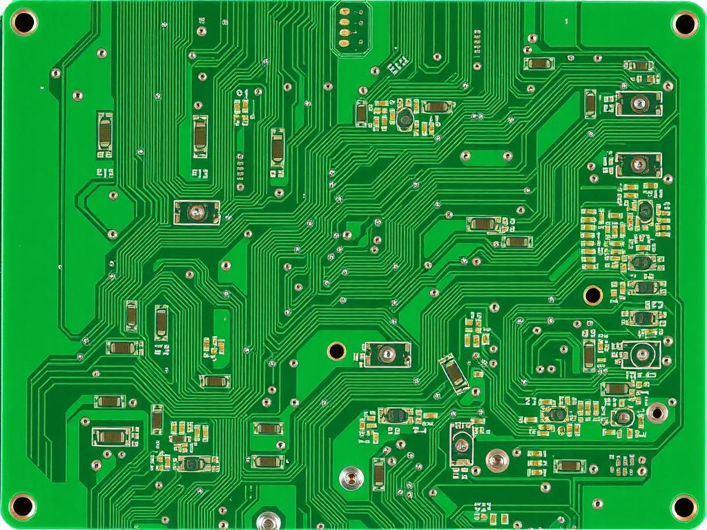
In my 20 years in this industry, I’ve seen countless pcbs go through the depaneling process. Simply put, depaneling is the process of separating individual pcbs from a larger panel or multiblock. Imagine a sheet of stamps – you print them all together for efficiency, then separate them. It’s the same principle with pcbs. During pcb panelization, we group many smaller individual pcbs together on a single panel for efficient manufacturing and surface mount technology (SMT) processes. This allows us to handle many boards at once, drastically increasing throughput. However, these interconnected pcbs need to be separated into the individual pcbs that will be used in the final product. This process step in high-volume electronics assembly is critical because the method used for depaneling directly impacts the quality and reliability of the final electronic devices. Incorrect depaneling can stress the board, damage components, or even breaks the pcb.
Exploring the Router Method: Achieving Precise and Efficient PCB Separation?
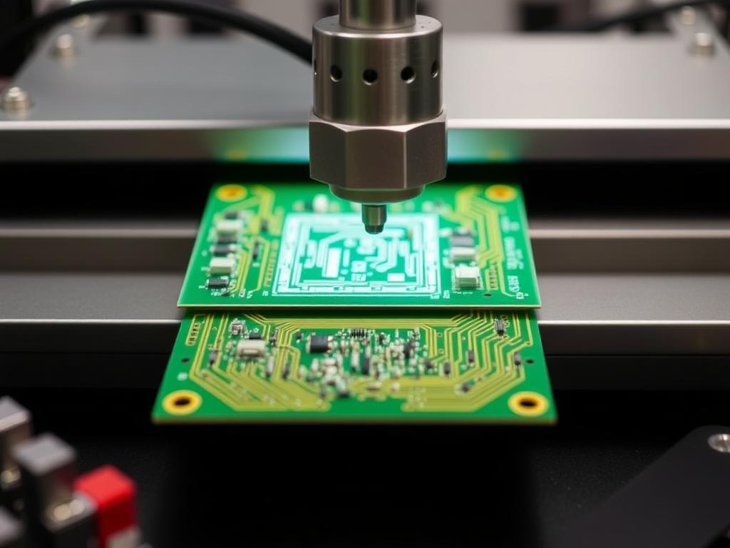
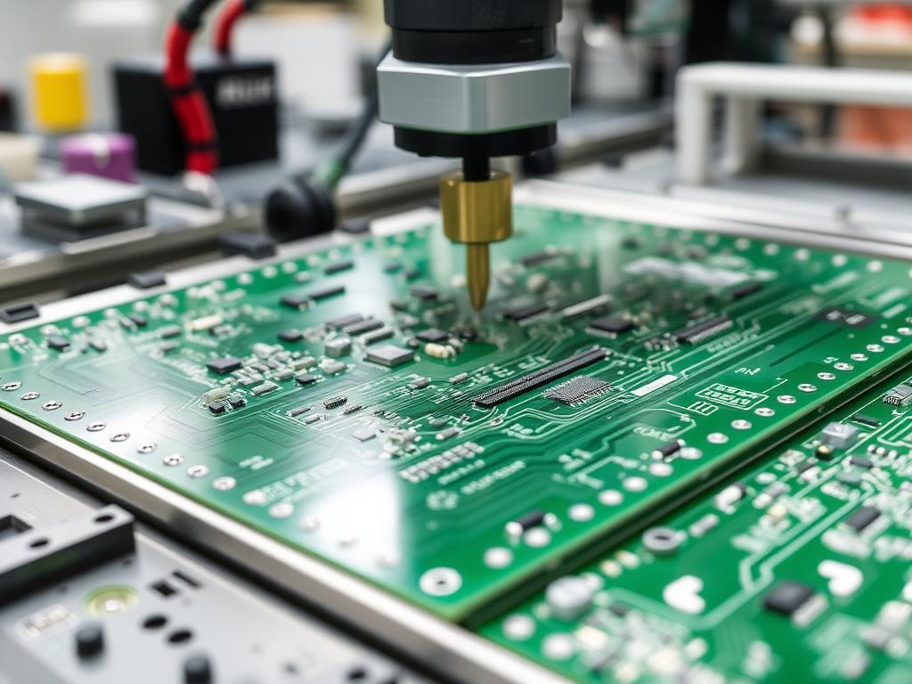
The depaneling router is a machine that uses a router bit to precisely cut the pcb along pre-scored lines or designated paths. Think of it like a miniature CNC machine specifically designed for pcb separation. As someone intimately familiar with PCB Router Machine technology, I can attest to its versatility and accuracy. The router bit to mill the material of the tab connecting the individual pcbs is carefully controlled, often with the help of a special fixture or a vacuum holding system is used. This ensures a clean and stress-free separation. While the speed might not be the absolute fastest, the precision offered by routing makes it ideal for pcb designs where high precision is paramount and for various pcb materials. We’ve seen incredible advancements in router technology over the years, leading to higher speeds and greater automation. Consider our GAM 380AT PCB Bottom Depaneling Machine, a prime example of a robust and reliable depaneling router.
The Advantages of Laser Depaneling: When is Laser Technology the Best Choice?
Laser depaneling has emerged as a cutting-edge depaneling method, particularly when high accuracy and minimal stress are paramount. As experts in PCB Laser Depaneling, we’ve seen firsthand how laser technology provides a non-contact method of separating the individual pcbs. A focused laser beam precisely vaporizes the pcb material, resulting in clean edges and minimal stress on sensitive components. This is particularly beneficial for thin and flexible pcbs, as well as those with densely populated components. The precision offered by laser depaneling is unmatched, allowing for intricate shapes and tight tolerances. While the initial investment might be higher compared to other methods, the benefits in terms of quality and reduced stress make it a compelling choice for many applications. Our DirectLaser H1 High-Precision Laser Cutting Machine showcases the pinnacle of laser technology for pcb separation. The advantages of laser depaneling truly shine when dealing with delicate or complex pcb designs.
Understanding V-Groove Depaneling: A Cost-Effective Solution for Certain PCBs?
V-Groove depaneling, also known as scoring, is a cost-effective depaneling method often used for pcbs with straight lines and simple designs. This two-part process involves creating a V-shaped groove on both sides of the pcb along the intended separation lines. The operator simply breaks the pcb along these weakened lines, either manually (hand depaneling) or with the assistance of a dedicated machine. While it offers a higher throughput compared to routing, it’s crucial that the pcb must be designed specifically for this method. The pcb thickness and the depth of the V-groove are critical factors in ensuring a clean break without damaging the components. As experts in V-Groove Depaneling, we offer solutions like the ZM30-P PCB Guillotine Separator, which provides a controlled and efficient way to separate V-grooved pcbs. This method is suitable for strain-resistant circuits.
Exploring the Punch Method: High-Throughput Depaneling for Specific Applications?
Punching is a process where single pcbs are punched out of the panel using a custom-made die. This depaneling method is characterized by its exceptionally high throughput, making it ideal for high-volume production of relatively simple pcb designs without smd components. Imagine stamping out cookies – the punch method works on a similar principle. The entire pcb is separated in a single action, making it incredibly fast. However, the tooling cost for creating the custom die can be significant, and this method is generally limited to simpler shapes. While it offers speed, the stress imparted on the pcb during the punch process needs careful consideration. Our ZM10T & 15T PCB & FPC Punching Cutting Machine represents our capability in providing robust punch solutions for specific high-volume applications. This method is often used to separate panels into smaller ones.
How Does PCB Panelization Influence the Choice of Depaneling Method?
PCB panelization plays a significant role in selecting the right depaneling method. The way pcbs are arranged on the larger panel and the type of connection methods used (e.g., tabs with routing, V-grooves, or direct connection for punching) directly dictate which depaneling solution is most appropriate. For instance, pcbs connected with perforated tabs are often separated using a router, which precisely mills away the material of the tab. Pcbs with V-grooves are designed for separation via a blade or manual breaking. Understanding the initial pcb panelization strategy is crucial for ensuring a smooth and efficient depaneling process. Careful consideration of pcb panelization during the design phase can significantly impact the efficiency and cost-effectiveness of the subsequent depaneling stage.
What is the Typical Throughput of Different PCB Depaneling Systems?
The throughput of a depaneling system is a critical factor, especially in high-volume electronics assembly production. Punch methods generally offer the highest throughput, as entire pcbs are separated in a single action. Router systems offer good throughput, especially with advancements in automation and multi-tool heads, allowing for multiple pcbs to be depaneled simultaneously. Laser depaneling, while highly precise, might have a lower throughput compared to punch methods, but it excels in handling complex shapes and delicate materials where speed isn’t the only priority. V-groove depaneling offers a mid-range throughput, depending on the level of automation. Choosing the right depaneling method involves balancing throughput requirements with factors like precision, cost, and material compatibility. We understand the need to increase the throughput of printed circuit board production and offer various solutions to meet those demands.
Key Considerations When Selecting the Right Depaneling Method for Your PCBs?
Selecting the right depaneling method is a crucial decision that impacts both the efficiency and quality of your pcb production. Several factors need careful consideration. The pcb material and pcb thickness are important, as some methods are better suited for certain materials than others. The complexity of the pcb designs and the presence of sensitive components will influence whether a low-stress method like laser depaneling is necessary. The required throughput and budget constraints are also key factors. For high-volume production of simple designs, punch methods might be the most cost-effective, while for intricate and sensitive pcbs, laser depaneling might be the preferred choice. Ultimately, the best depaneling method is the one that balances your specific requirements for precision, speed, cost, and material compatibility. Our team can help you navigate these considerations to ensure optimal results for your depaneling process.
Best Practices for Ensuring a Smooth and Efficient PCB Depaneling Process?
Ensuring a smooth and efficient depaneling process involves more than just choosing the right equipment. Best practices include proper pcb panelization design, taking into account the chosen depaneling method. Regular maintenance of your depaneling machines is crucial to prevent downtime and ensure consistent performance. Proper training for operators is essential to minimize errors and maximize efficiency. For routing, using the correct router bit and maintaining its sharpness is vital to prevent damage and ensure clean cuts. For laser depaneling, proper alignment and maintenance of the laser beam are critical. Implementing quality control checks throughout the depaneling process can help identify and address issues early on. By adhering to these best practices, you can optimize your depaneling process, reduce costs, and ensure the delivery of high-quality depaneled pcbs.
The Future of Depaneling: Automation and Advanced Technologies?
The future of depaneling is undoubtedly intertwined with increased automation and the adoption of advanced technologies. We are seeing a growing demand for fully automated depaneling systems that can seamlessly integrate into existing production lines, such as our SMT In-Line Depaneling Machine Solution. This includes robotic arm integration for loading and unloading pcb panels, further enhancing throughput and reducing manual intervention. Advancements in laser technology are leading to faster and more precise laser depaneling systems. The focus is on developing depaneling solutions that offer greater flexibility, higher precision, and increased efficiency to meet the evolving demands of the electronics industry. As a leader in depaneling technology, we are committed to driving these innovations and providing our customers with cutting-edge solutions for their pcb separation needs.
Ready to Optimize Your PCB Depaneling Process?
With my two decades of experience, I’ve witnessed the evolution of depaneling from a manual task to a highly sophisticated and automated process. Whether you’re dealing with the intricacies of laser depaneling, the precision of routing, or the high throughput demands requiring a punch, we have the expertise and equipment to help. Our depaneling machines are designed for precise and efficient pcb separation, ensuring the quality and reliability of your final products.
Our reputation as the world’s leading PCB depaneling machine manufacturer is built on trust and performance, which is why industry giants like TP-LINK, Canon, BYD, Flex, TCL, Xiaomi, Lenovo, OPPO, HONOR, and Foxconn rely on our solutions. We understand the critical nature of the depaneling process step in high-volume electronics assembly and offer a comprehensive range of equipment to meet diverse needs.
Don’t let inefficient depaneling slow down your manufacturing process. Contact us today to discuss your specific requirements and discover how our advanced depaneling solutions can enhance your throughput and product quality. Whether you need a standalone depaneling router is a machine or a fully integrated automation system, we’re here to guide you toward the optimal depaneling method.
Frequently Asked Questions about PCB Depaneling
What is the difference between routing and laser depaneling? Routing uses a router bit to mill the material of the tab, while laser depaneling uses a laser beam used for cutting the pcb. Laser depaneling offers high precision and low stress, while routing is versatile for various materials and thicknesses.
Is the punch method suitable for pcbs with surface mount components? Generally, the punch method is not recommended for pcbs with surface mount components due to the high stress involved, which can damage the components.
How can I improve the throughput of printed circuit board depaneling in my factory? Consider implementing automated depaneling systems, optimizing pcb panelization, and ensuring regular maintenance of your depaneling machines.
What are the key factors in selecting the right depaneling method? Factors include pcb material, pcb thickness, pcb designs complexity, required throughput, and budget.
What kind of maintenance is required for depaneling machines? Maintenance varies depending on the depaneling method but typically includes cleaning, lubrication, and regular inspection and replacement of cutting tools or laser components.
Key Takeaways:
- Depaneling is a critical process step in high-volume electronics assembly for separating individual pcbs.
- Various depaneling methods exist, including routing, laser depaneling, V-groove, and punch, each with its advantages and disadvantages.
- Selecting the right depaneling method depends on factors like pcb material, design complexity, and throughput requirements.
- Automation is increasingly important for enhancing efficiency and throughput in depaneling.
- Proper pcb panelization and adherence to best practices are crucial for a smooth depaneling process.
Let us help you optimize your pcb separation process. Contact us today to learn more about our depaneling solution!