![]()

PCB depaneling for electronics companies
Precision PCB Depaneling: Harnessing the Power of Laser and Other Advanced Methods for Efficient Circuit Separation
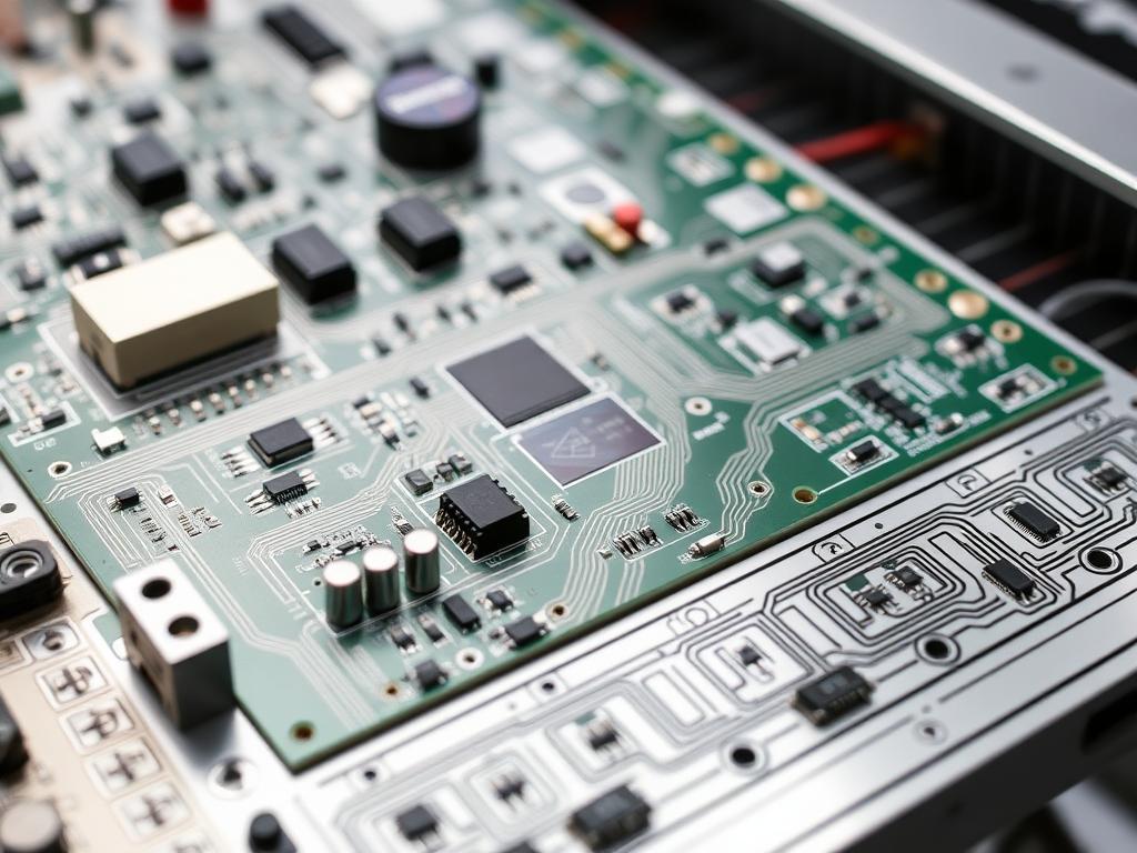
The process of pcb depaneling, separating individual pcbs from a larger manufactured panel, is a crucial step in electronics manufacturing. This article explores the various methods of pcb separation, with a particular focus on the precision and efficiency offered by laser technology. Understanding these techniques is vital for anyone involved in the production of electronics, whether you’re a large manufacturer or an individual enthusiast. Read on to discover how the right pcb depaneling equipment can optimize your workflow and ensure the quality of your final product.
Understanding PCB Depaneling: Choosing the Best Method for Your Circuit Boards
With two decades navigating the intricacies of pcb fabrication, I’ve witnessed firsthand the evolution of depaneling methods. Let’s delve into some common questions surrounding this vital stage in the manufacturing process.
What are the Primary Depaneling Methods Used in PCB Manufacturing?
The process of removing individual printed circuit boards from a larger panel, often referred to as an array, involves several distinct techniques. These depaneling methods vary in their approach, cost, and suitability for different types of pcbs. Common methods include:
- Laser Depaneling: Utilizing a focused laser beam to vaporize the material and separate the pcbs. This is known for its precision and minimal stress.
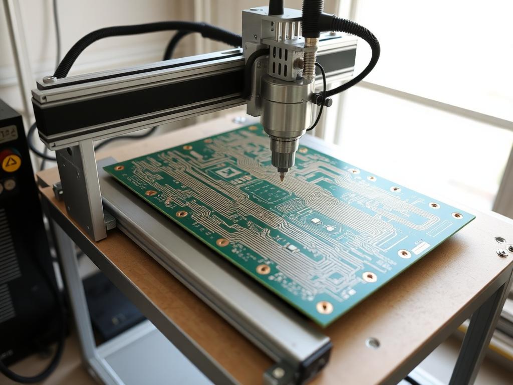
- Routing: Employing a high-speed router with a specialized bit to mill along predefined cut lines.
- V-Scoring (or V-Cut): Involves creating V-shaped grooves along the cut lines, allowing the pcbs to be snapped apart.
- Punching: Using a specialized tool to punch out the individual pcbs.
- Saw Cutting: Employing a saw to separate the pcbs.
The choice of method used significantly impacts the quality of the separated boards, the throughput of the manufacturing process, and the potential for mechanical stress. At our facilities, we utilize a range of these methods, allowing us to tailor the cutting process to the specific needs of our clients, from high-volume smt assembly to specialized flex pcb applications.
Why is Laser Depaneling Increasingly Preferred for Modern PCB Manufacturing?
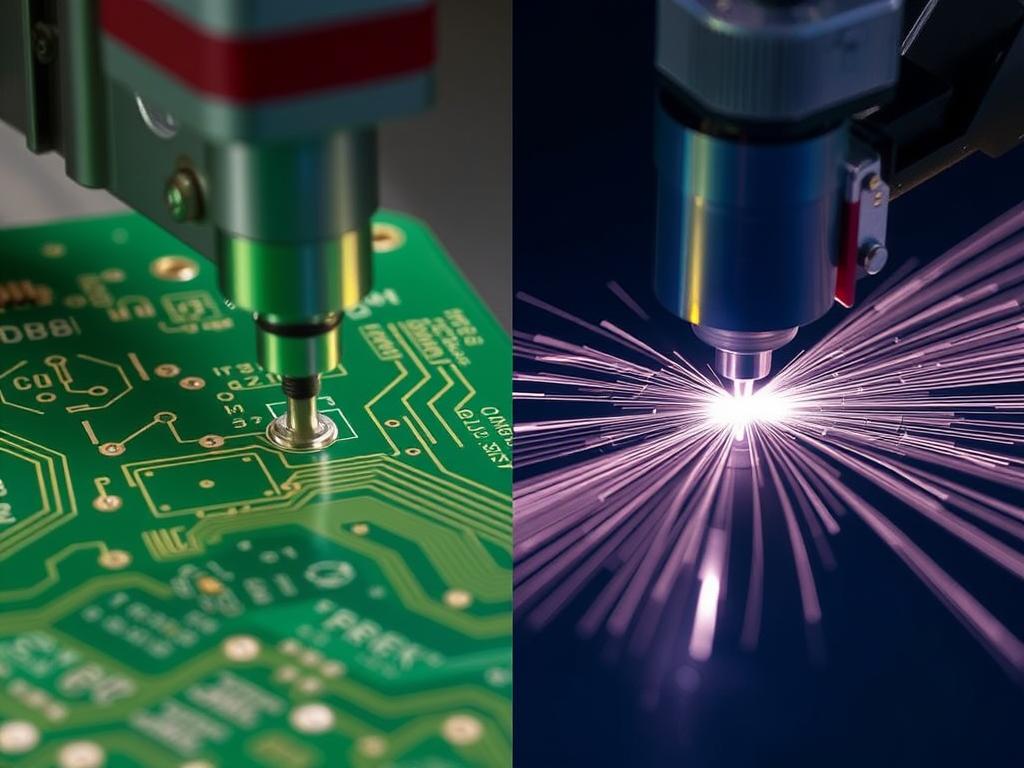
Laser depaneling has become a cornerstone of modern pcb manufacturing due to its numerous advantages. The primary benefit lies in its precision and minimal impact on the circuit. Laser cutting, being a non-contact cutting method, eliminates mechanical stress, which is crucial when working with delicate sensitive components or thin substrates like those found in flex pcbs. The focused laser beam allows for intricate and complex cut lines that are difficult to achieve with traditional mechanical methods. Furthermore, laser depaneling offers a cleaner cutting process, minimizing dust and debris, which is essential for maintaining cleanliness in the electronics production environment. Thanks to its precision and efficiency, laser depaneling significantly contributes to increased throughput without compromising the integrity of the pcbs. Our PCB Laser Depaneling services are highly sought after for these very reasons, particularly by manufacturers of electronic devices like smartphones and wearables.
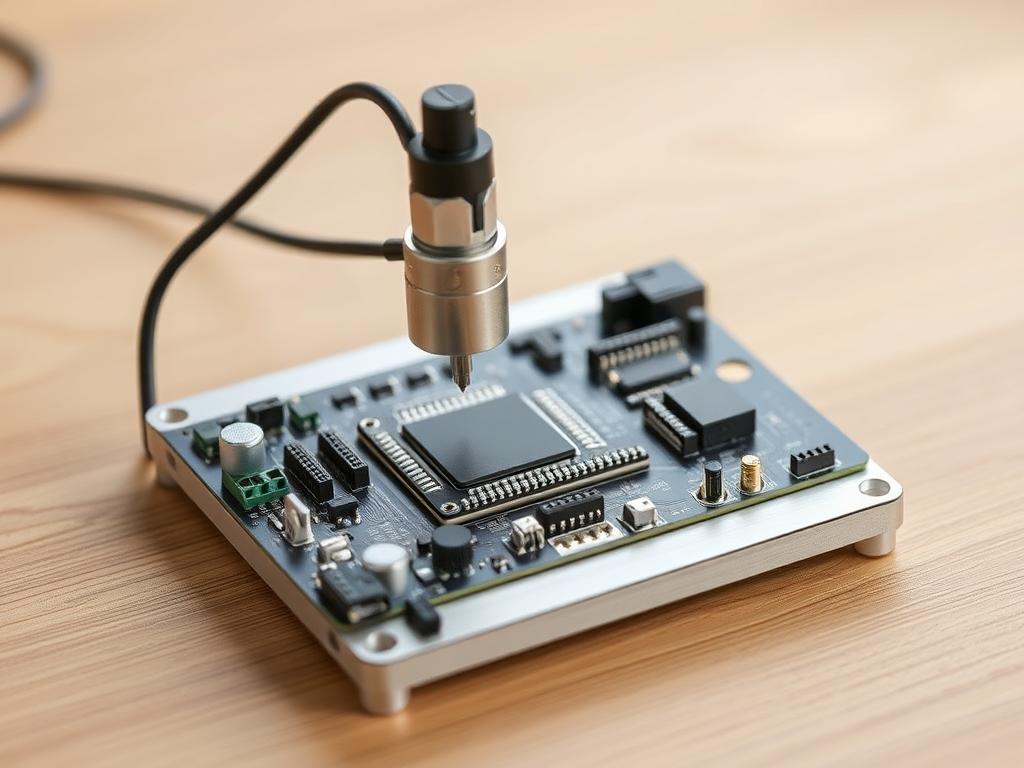
How Does Laser PCB Depaneling Equipment Ensure Precision and Minimize Stress?
Laser pcb depaneling equipment operates by directing a highly focused laser beam onto the pcb substrate. The energy from the laser vaporizes the material along the programmed cut line, effectively separating individual printed circuit boards. The precision is controlled by sophisticated software and motion systems, ensuring the laser beam follows the exact contours defined in the design. The key to minimizing mechanical stress lies in the non-contact nature of the cutting process. Unlike mechanical methods that apply force, the laser interacts with the material without physical contact, eliminating the risk of bending, flexing, or otherwise stressing the circuit. This is particularly important for thin and fragile flex pcbs or boards with delicate surface mount components. Our pcb depaneling equipment, including our advanced uv laser systems, is designed to deliver this level of precision and care, making us a preferred choice for pcb manufacturing.
What are the Advantages of Using a UV Laser for PCB Depaneling?
While various types of lasers can be used for pcb depaneling, the uv laser offers distinct advantages, especially when working with fr4 and other common pcb materials. UV lasers operate at a shorter wavelength, which results in a smaller focused spot size and a narrower cut kerf. This finer laser beam translates to higher precision and a cleaner cut with less material affected by the heat. The shorter wavelength also means the uv laser is readily absorbed by common pcb materials, leading to more efficient material removal and faster cutting speeds. This efficiency not only increases throughput but also minimizes the heat-affected zone, further reducing the risk of damage to sensitive components. Our laser pcb depaneling capabilities heavily rely on uv laser technology to ensure the highest quality and precision for our clients.
When Might Other Depaneling Methods Like Routing or V-Scoring Be More Suitable?
Despite the advantages of laser depaneling, other depaneling methods like routing or v-scoring remain relevant for specific applications. Routing, using a specialized depaneling machine, is often a more cost-effective solution for pcb cutting, especially for thicker boards or large quantities where the capital investment for high-end laser equipment might not be immediately justifiable. V-scoring is another cost-effective method suitable for pcbs with straight lines and when some degree of mechanical stress is acceptable. It’s particularly useful for pcbs that will be populated with less sensitive components. The choice of cutting method often depends on factors like production volume, board thickness, component sensitivity, and budget. While laser offers superior precision and reduced stress, router and v-scoring can be practical and efficient for certain types of pcb manufacturing.
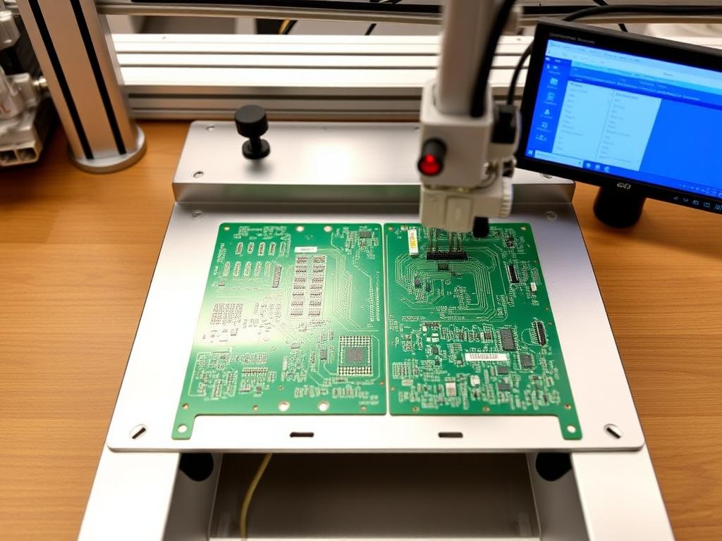
How Does Automation Enhance Efficiency in PCB Depaneling Processes?
Automation plays a crucial role in optimizing the depaneling process and maximizing throughput. Automated pcb depaneling equipment can handle the process of separating pcbs from the larger panel with minimal human intervention. This includes automated loading and unloading of pcb panels, precise control of the cutting process (whether laser cutting or routing), and often integrated inspection systems to ensure quality. Automation not only increases cutting speed and throughput but also reduces the risk of human error, leading to more consistent and reliable results. For high-volume pcb manufacturing, automation is essential for maintaining efficiency and meeting production demands. Our pcb equipment includes a range of automated solutions designed to streamline the depaneling process for our clients.
What Factors Determine the Cutting Speed and Throughput of Different Depaneling Methods?
The cutting speed and throughput of different depaneling methods are influenced by several factors. For laser depaneling, the power of the laser, the type of laser (uv or co2), the material and thickness of the pcb, and the complexity of the cut line all play a role. Routing speed is determined by the spindle speed, the feed rate, and the type of cutter used. V-scoring throughput is largely dependent on the manual process of separating the multiple boards. Generally, laser depaneling offers high cutting speeds for intricate designs and thin materials, while routing can be faster for simpler cuts on thicker boards. Automation can significantly boost the throughput of any cutting process by reducing handling time and ensuring continuous operation. When selecting pcb depaneling equipment, it’s crucial to consider the required throughput and choose a method in practice that can meet those demands efficiently.
Why is Fixture Design Important for Accurate PCB Depaneling?
Proper fixture design is critical for ensuring accurate and consistent pcb depaneling, regardless of the cutting method used. The fixture securely holds the pcb panel in place during the cutting process, preventing movement or vibration that could compromise the accuracy of the cut line. A well-designed fixture will also provide adequate support to prevent flexing, especially when using mechanical methods like routing. For laser depaneling, the fixture needs to be designed to avoid interference with the laser beam and to allow for proper ventilation of any fumes produced. Investing in high-quality, custom-designed fixtures is essential for achieving precise and reliable pcb cutting and minimizing the risk of damage to the pcbs.
Considering Future Trends: What Innovations are Shaping PCB Depaneling?
The field of pcb depaneling is continuously evolving, driven by the increasing complexity and miniaturization of electronics. Future trends point towards even greater adoption of laser technology, with advancements in laser sources and control systems leading to faster cutting speeds and improved precision. We can also expect to see more sophisticated automation and integration of depaneling equipment into fully automated smt lines. There’s also a growing focus on developing more flexible and adaptable depaneling methods that can handle a wider range of pcb materials and designs. The demand for cleaner cuts, reduced mechanical stress, and higher throughput will continue to drive innovation in this critical aspect of pcb manufacturing. We are actively involved in researching and implementing these emerging technologies to provide our clients with the most advanced and efficient pcb depaneling equipment available.
Frequently Asked Questions About PCB Depaneling
What is the main advantage of laser depaneling over mechanical methods? The primary advantage is the elimination of mechanical stress, making it ideal for sensitive components.
Which depaneling method is most cost-effective for large quantities of simple pcbs? V-scoring is often the most cost-effective for high-volume production of simple designs.
What is the role of a fixture in the pcb depaneling process? The fixture securely holds the pcb panel during cutting, ensuring accuracy and preventing damage.
Why is cleanliness important in pcb depaneling? Maintaining cleanliness minimizes contamination and ensures the reliability of the electronic devices.
Can different depaneling methods be combined in a single production line? Yes, depending on the specific needs, different methods can be integrated for optimal efficiency.
Key Takeaways for Efficient PCB Depaneling
- PCB depaneling is the process of separating individual pcbs from a larger panel.
- Laser depaneling offers high precision and minimizes mechanical stress.
- Routing is a cost-effective option for thicker boards.
- V-scoring is suitable for large quantities of simple designs.
- Automation significantly enhances throughput and consistency.
- Proper fixture design is crucial for accuracy.
With 20 years of experience in the pcb depaneling industry, we understand the critical role this cutting process plays in the overall success of electronics manufacturing. Whether you require the precision of laser pcb depaneling, the robustness of traditional routing, or other specialized pcb equipment, we offer solutions tailored to your specific needs. Our commitment to innovation ensures that you have access to the most advanced methods of pcb separation available. From flex pcbs to complex multilayer boards, our expertise and pcb depaneling equipment guarantee efficient and high-quality results. Manufacturers are listed on pcb directories for a reason – experience and reliability matter. Get a quote today and discover how our pcb depaneling equipment can optimize your manufacturing process.