![]()


PCB depaneling for consumer electronics
Precision PCB Depaneling: A Comprehensive Guide to Cutting-Edge Methods
As someone who’s spent the last 20 years in the thick of the PCB industry, I’ve seen firsthand how critical the depaneling process is. Separating individual printed circuit boards (PCBs) from a larger panel might seem like a simple step, but it’s actually a crucial stage that demands precision and the right tools. This article will explore the various methods of PCB depaneling, from manual techniques to state-of-the-art laser cutting, and help you choose the best approach for your specific needs. You’ll learn why the right choice here can affect everything from component integrity to overall production efficiency. So, whether you’re a large electronics manufacturer or a lone PCB enthusiast, understanding the nuances of depaneling is essential for success.
Detailed Explanation
1. What exactly is PCB Depaneling and why is it so important?
PCB depaneling, also called singulation, is the process of separating individual printed circuit boards from a larger panel after the assembly and soldering processes. It’s a critical step in manufacturing electronic devices, as the pcbs are often produced in a larger panel to improve the efficiency of production and assembly. Why is it so important? Well, the chosen method has a direct impact on the quality, reliability, and yield of the final product. A poorly executed depaneling process can induce unwanted mechanical stress, potentially damaging sensitive components or the printed circuit traces, leading to functional issues and higher production costs. If you fail at this step, the product will fail – it’s that simple. For more insight into the world of PCB manufacturing, this guide provides more information, PCB Manufacturing: A Comprehensive Guide.
The ultimate goal of the depaneling process is to separate individual pcbs cleanly and accurately without causing damage. This requires choosing the right depaneling tool and method that matches the characteristics of the circuit board, the type of components mounted, and the overall manufacturing requirement. This isn’t just about separating panels, it’s about maintaining quality, reducing waste, and ensuring the proper functionality of the final electronic device.
2. What are the traditional methods of PCB depaneling?
Traditional methods of pcb depaneling often involve manual separation techniques or the use of simple tools. These manual methods may involve using a hand cutter or breaking the pcbs along pre-scored lines. While these methods are generally cost-effective for small-scale operations, they have significant drawbacks. Manual depaneling can introduce mechanical stress, leading to bending or twisting of the board, potentially damaging sensitive components, especially in flexible circuits. Additionally, they are not suitable for boards with surface mount components near the edges. Also, the quality and precision can vary significantly due to the inconsistencies of human handling. As someone who’s spent considerable time in the PCB shop, I can attest that consistent and reliable separation using manual methods is almost impossible.
Another common traditional approach is the use of a die. This involves pressing a specialized die against the panel to separate the pcbs. While this method can achieve faster separation than fully manual methods, it still introduces significant mechanical stress. Additionally, the initial cost of creating a specific die for each different pcb design can be high. The limitations of these traditional approaches highlight the need for more advanced and precise solutions for modern electronic production. These methods, while seemingly simple, often lack the precision and consistency required for today’s high-density and sensitive components.
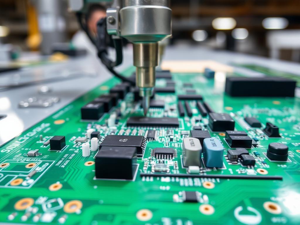
3. What is laser depaneling, and what are its benefits?
Laser depaneling, a cutting-edge method, utilizes high-precision laser beams to cleanly and accurately separate pcbs from the panel. One of the major benefits of laser depaneling is the minimal mechanical stress it imparts on the circuit board. Unlike manual methods or die cutting, laser depaneling doesn’t physically contact the board, reducing the risk of damage to delicate components, especially on flexible boards. This leads to better reliability and higher yield.
Furthermore, laser cutting provides exceptional flexibility and accuracy. It can handle complex shapes and very precise cutting paths that are impossible with traditional tools. The laser beam’s fine cutting capability allows separation of pcbs with minimal clearance, enabling higher panel utilization and savings. Laser systems are also highly adaptable and can be easily reconfigured for different pcb designs, making it a very cost-effective solution in the long run. In my experience, switching to laser depaneling has consistently resulted in more efficient and higher-quality results for many of our clients.
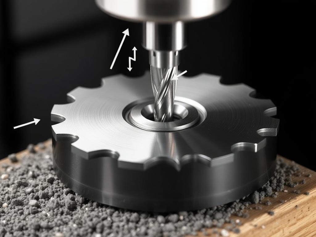
4. How does router depaneling compare to other methods?
Router depaneling, also known as pcb routing, employs a high-speed milling cutter to separate pcbs from a panel. This method is particularly suitable for handling thicker pcbs and for cutting complex contours. The main advantage of router depaneling is its versatility in cutting different materials and thickness levels. It’s a good option when the requirement is for clean edges, and it can handle more complex board shapes than a simple V-cut.
However, router depaneling also has some drawbacks. It does generate dust and debris, which might require additional cleaning steps after the depaneling process. Also, while modern router systems are designed to minimize mechanical stress, it is still higher compared to laser depaneling. The milling cutter applies some force to the board, potentially inducing stress, especially on flexible circuit boards or pcbs with delicate surface mount components. While router depaneling is a step up from manual methods, laser cutting has become the go-to choice when high precision and minimal stress are paramount. To learn more, see PCB Separation Techniques:Routing vs. Laser Cutting
5. What is V-Groove Depaneling and when should it be used?
V-Groove depaneling is a method that employs a V-shaped blade to score the panel along the lines where the individual pcbs need to be separated. Once the v-score is made, the individual panels can be broken apart manually or by mechanical means. This method is often used when the pcbs are relatively simple in shape and when the separation line is a straight line. V-Groove is a cost effective method for a high volume production, especially when dealing with rigid fr4 boards.
While cost-effective, V-Groove depaneling has limitations. It’s not suitable for pcbs with components located very close to the breaking line due to the risk of damage. Also, the separation is not always as clean as with laser cutting or router methods, and it can introduce some level of mechanical stress to the board. Therefore, V-Groove is suitable for situations where cost efficiency and high-volume is critical, and where the pcbs layout and components allow for this type of separation. In my experience, if the design allows and the components are placed carefully, it’s an efficient option to separate panels. Our ZM30-P PCB Guillotine Separator is an example of V-groove depaneling solution that can be used in conjunction with manual panel breaking.
6. Why might you consider a PCB/FPC Punching Machine for depaneling?
A PCB/FPC punching machine uses a die to stamp out individual circuits from a panel. This method is especially suitable for flexible printed circuit boards (FPCs) and other materials where precise and fast separation is required. It can quickly punch out individual pcbs with consistent accuracy, especially when you have large production runs with standardized shapes and sizes.
However, the upfront cost of creating a custom die can be significant, and it’s not economical for small production runs or for diverse pcb designs. In many cases, you will require a unique die for every design, which can limit flexibility. However, once in place, it’s very efficient and very quick to separate pcbs from the panel. I often recommend this when the manufacturing process involves many of the same types of pcbs and high throughput is a critical requirement. If you need more information, our ZM10T & 15T PCB & FPC Punching Cutting Machine is a great example of this technology in action.
7. What is the impact of mechanical stress during the depaneling process?
Mechanical stress is a significant concern during the depaneling process. It refers to the physical forces applied to the board during separation, whether by bending, twisting, cutting, or punching. This stress can induce unwanted changes in the pcb and its delicate components. It can cause micro-cracks in the substrate, damage surface mount components, or sever thin copper traces. All these problems can lead to decreased reliability, reduced yield and overall product failure.
Minimizing mechanical stress is critical for ensuring the functionality and reliability of electronic devices. This is why methods such as laser depaneling are becoming more popular, as they practically eliminate mechanical contact and thus reduce the risk of inducing stress. Choosing a depaneling method with minimal stress is not just about preserving the physical integrity of the board but also about ensuring the long-term performance of the final product. In my experience, paying extra attention to this factor can drastically reduce defects and improve overall quality.
8. What applications benefit most from laser PCB depaneling?
Laser depaneling offers many advantages that make it particularly suitable for specific applications. Firstly, it’s the go-to choice for flexible circuit boards and flexible printed circuit boards (FPCs). These boards are very sensitive to mechanical stress, which traditional methods can’t handle without risk. Secondly, laser depaneling is ideal for high-density pcbs that have very small and complex designs. High precision of laser allows to cut close to sensitive components without causing damage. It is also ideal for a wide variety of pcb materials including FR4, ceramic, and composites.
Additionally, industries like aerospace, medical devices, and high-performance electronics, where reliability and minimal damage are paramount, heavily rely on laser cutting. The ability to precisely separate pcbs with minimal stress and high accuracy ensures that the performance of the final product is not compromised. This is why it is used by most well known brands that have high quality requirement, like the ones listed earlier such as TP-LINK, Canon, BYD, Flex, TCL, Xiaomi, Lenovo, OPPO, HONOR and Foxconn. Laser depaneling truly shines where precision, minimal impact and high reliability are needed.
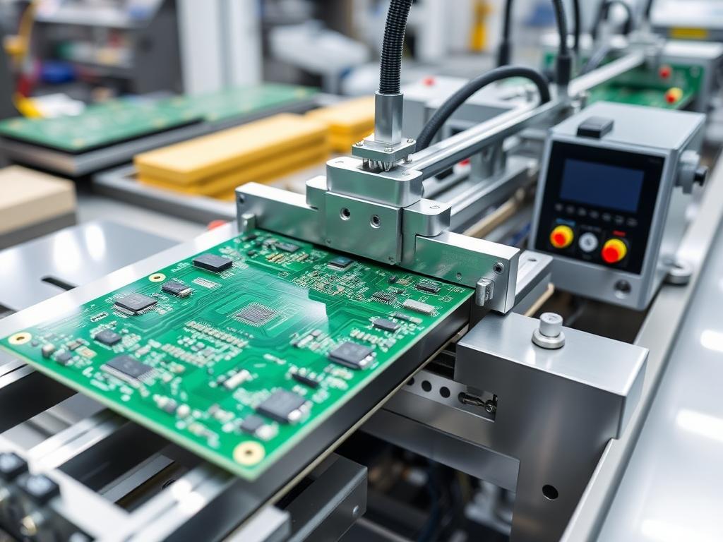
9. How can we help you optimize your depaneling process?
With 20 years of experience in the PCB industry, we at PCB Depaneling understand the complexities of the depaneling process and we’re ready to offer customized solutions for all your needs. Whether you’re dealing with rigid or flexible circuit boards, or high volume production or individual prototypes we have the right tools and expertise to guide you. We offer a comprehensive range of equipment, including laser depaneling systems, router machines, and various other methods, including V-Groove Depaneling and PCB/FPC Punching Machines to meet your specific needs.
Our experts are here to work with you to assess your specific requirements, from board design to required throughput and quality. We are committed to providing solutions that not only improve your production efficiency but also enhance the reliability of your products. We can assist you in choosing the best method, whether it’s automating your line using our Automatic Equipment or creating a more integrated SMT whole line equipment solution. In addition to that we provide accessories that you might need in the depaneling manufacturing process. Don’t hesitate to contact us so we can explore how we can help you to achieve excellence in PCB manufacturing.
10. What are some common questions about PCB depaneling?
- What is the difference between laser depaneling and router depaneling? Laser depaneling utilizes a laser beam to cut, offering high precision and minimal mechanical stress, ideal for sensitive pcbs and flexible circuit boards. Router depaneling uses a milling cutter, suitable for thicker pcbs and more complex shapes, but may induce more stress.
- Is manual depaneling a suitable method for all types of boards? Manual depaneling is often cost-effective for small-scale operations but is not suitable for sensitive components or boards that require high precision. It can introduce mechanical stress and is not suitable for surface mount components or flexible circuit boards and it is not optimal for large volumes of pcbs.
- How can I choose the right depaneling method for my production line? Selecting the right method depends on various factors including the type of pcbs, their size, required precision, volume and component placement. Laser depaneling is excellent for intricate designs, while router depaneling is suited for thicker boards, and V-Groove is good for larger volume when suitable.
- What is the long-term benefit of using laser depaneling? Laser depaneling leads to reduced mechanical stress, enhanced precision, and higher yield. While the initial investment might be more significant, you’ll see cost savings in the long run due to less damage and higher reliability. Also, the flexibility of laser systems will allow you to change the separation requirements easily.
- Can laser depaneling handle flexible and rigid boards equally well? Laser depaneling can handle both rigid and flexible boards, but it is especially advantageous for flexible boards because it introduces very little mechanical stress, which is critical for these sensitive materials.
Key Takeaways
- PCB depaneling is a vital process that significantly impacts the quality and reliability of electronic devices.
- Various depaneling methods exist, ranging from manual to advanced laser cutting, each with its own benefits and drawbacks.
- Laser depaneling is the most accurate and least stress inducing option, suitable for sensitive components and flexible circuit boards.
- Router depaneling is a good option for thicker boards and more complex shapes, while V-Groove is suitable for high-volume straight line separation.
- Choosing the right depaneling method depends on the specific requirements of your pcbs and overall production needs.
- Minimizing mechanical stress during the depaneling process is crucial for preserving the functionality and reliability of the final product.
- We are here to assist you in optimizing your process and provide the best solution for your specific needs.
- Contact us to discover how our expertise and comprehensive equipment range can enhance your PCB production process.
By understanding these key aspects of PCB depaneling, you can make informed decisions that lead to higher quality products and more efficient manufacturing processes.