![]()

PCB Laser Depaneling for Medical Electronics: Eliminate Microcracks in Critical Applications
When we walk onto the factory floor of a high-reliability electronics manufacturer—whether they are building wearable cardiac monitors, neural implants, or portable ultrasound diagnostic tools—we always look for one specific thing immediately: how exactly are they separating their finished circuit boards from the production panel?
Here is the direct answer and the ultimate solution to your yield rate problems: If your SMT line is currently relying on physical, mechanical separation methods to process medical-grade devices, you are introducing invisible mechanical stress into your assemblies. To entirely eliminate the risk of microcracks and easily comply with strict medical manufacturing standards like ISO 13485, you need to transition to a pcb laser cutting machine.
Why do we strongly recommend this? Because UV laser ablation is a 100% non-contact process. The immediate benefits are zero mechanical strain transferred to your delicate ceramic capacitors, a microscopic 25μm kerf width that saves expensive substrate material, and absolute technical cleanliness with zero fiberglass dust. In this comprehensive guide, we are sharing our extensive field experience to show you exactly why laser technology is the only secure choice for life-saving electronics, how you can start the transition, and the real-world data you need to justify the return on investment (ROI).
The Hidden Danger: Why Mechanical Depaneling Fails Medical PCBs
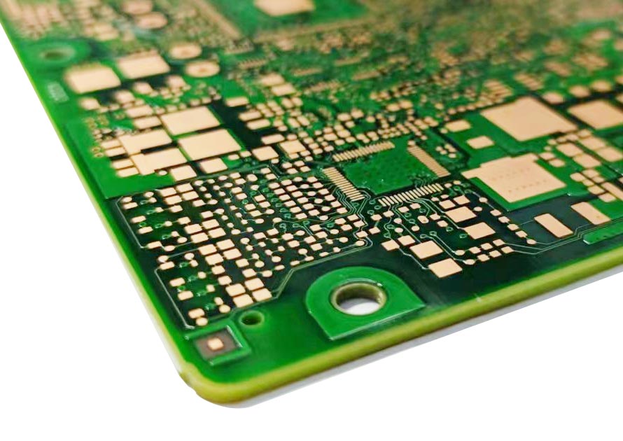
In the consumer electronics space, a dead circuit board means an RMA and a frustrated customer. In the medical electronics sector, a device failure can mean a compromised life. Look, in this business, “good enough” is a death sentence. We’re talking about medical PCBs—boards that are getting so thin and cramped it’s ridiculous. You’ve got BGAs, QFNs, and MLCCs practically hanging off the edge of the board. There’s zero room for error.
If you’re still messing around with a traditional or a standard , you’re playing with fire. That spinning bit or that wedging blade isn’t just cutting; it’s slamming mechanical vibration and bending strain right into the fiberglass. One tiny micro-crack in a capacitor and the whole board is junk—or worse, it fails in the field. You can’t leave that kind of risk to chance. Period.
This mechanical vibration causes microcracks in the solder joints and the components themselves. The terrifying part about microcracks is that they are virtually invisible during standard end-of-line Automated Optical Inspection (AOI). The medical device passes quality assurance, ships to the hospital or patient, and then fails months later due to normal thermal cycling or minor physical movement.
The Industry Data: According to a comprehensive industry analysis, an astonishing 12% of all PCB assembly defects can be traced directly back to the mechanical stress introduced during the depaneling process.
While a punching machine might be incredibly fast and economical for simple, low-cost rigid boards in the toy or basic appliance industry, the sudden, violent impact force of a punching die is completely unacceptable for fragile medical implants or flexible polyimide circuits (FPCBs).
How UV Laser Depaneling Solves the Microcrack Problem
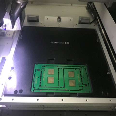
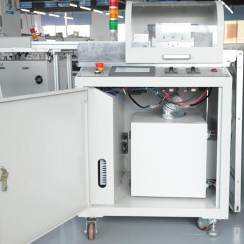
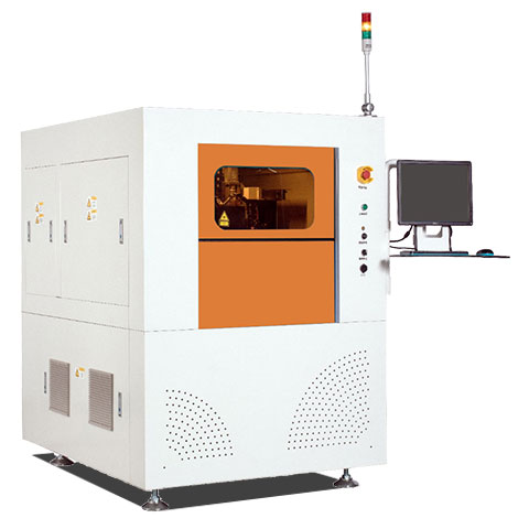
To eliminate these hidden defect costs, we consistently help EMS (Electronic Manufacturing Services) providers upgrade to a laser depaneling machine. Instead of grinding, snapping, or chopping through the fiberglass, a 355nm Ultraviolet (UV) laser vaporizes the FR4 and copper layers. This process is commonly known in the engineering world as “cold ablation.”
Core Benefits for Medical Manufacturing
1. Absolute Zero Mechanical Stress
Because no physical tool ever touches the circuit board during the laser cutting process, there is zero vibration and zero bending force. You completely eliminate the risk of fracturing delicate ceramic capacitors or breaking the microscopic solder spheres under a BGA.
2. Minimal Heat-Affected Zone (HAZ)
A common question we hear from process engineers is, “Won’t a laser burn the board?” The answer is no, provided you use the right technology. Advanced UV lasers utilize ultra-short pulse technology to limit thermal spread. In fact, studies show that the Heat-Affected Zone (HAZ) with UV lasers can be tightly controlled to less than 10 micrometers, compared to the 50-100 micrometers seen with older CO2 lasers. This ensures that sensitive components situated fractions of a millimeter away from the cut line remain completely safe.
3. Burr-Free & Dust-Free Cleanliness
Medical devices frequently require conformal coating to protect against bodily fluids, sterilization chemicals, or moisture. Mechanical routing leaves frayed fiberglass burrs and ionic residue that prevent the conformal coating from sealing properly. Laser ablation leaves a chemically clean, perfectly smooth edge. The vaporized material is immediately evacuated by localized vacuum extraction, completely removing the need for secondary, labor-intensive board-washing stations.
Best Practices: How to Start and Optimize Your Laser Process
Look, switching to laser tech isn’t some “plug-and-play” miracle fix. You don’t just buy the machine, hit a button, and walk away. If you want it to actually work, you’ve gotta rethink your whole panel layout and how the work flows through the shop.
We’ve been on the floor for dozens of medical-grade deployments, so we’ve seen what works and what’s a total waste of time. If you want to get this right the first time, here are the ground rules you need to follow to make sure the transition actually pays off.
Practice 1: Redesign Your Panels for Maximum Material Yield
How to Start: If you are migrating from mechanical routing, you need to stop leaving 2.0mm to 3.0mm routing channels between your individual boards.
The Benefit: A UV laser beam is incredibly thin—typically achieving cutting accuracies as tight as ±25 micrometers. This means you can push your individual PCBs right next to each other on the manufacturing panel, separated only by the microscopic laser kerf.
The Result: By switching to a laser system and updating their CAD layouts, we have seen engineering teams tighten their panel designs by up to 30%. When you are manufacturing medical-grade boards using expensive, specialized substrates like Liquid Crystal Polymer (LCP), Polyimide, or high-frequency Teflon, recovering 30% of your material in every single production run generates massive financial savings.
Practice 2: Match the Laser Wavelength to the Material
How to Start: Do not assume that one single type of laser will optimally cut every material in your factory.
Look, if you don’t understand the physics of how the laser actually hits the board, you’re gonna fry your components. It’s that simple.
If you’re cutting thick, old-school FR4 boards and you’ve got plenty of “breathing room” away from the components, a high-power CO2 laser is fine. It’s fast, it’s aggressive, and it gets the job done.
But once you start talking about medical rigid-flex, wearables, or those tight HDI boards, the game changes. You’ve gotta go with a UV Laser (355nm). Why? Because the UV laser doesn’t just “melt” the material like a blowtorch—it uses a photochemical process to snap the molecular bonds directly. That’s how you avoid carbonizing the edges or melting those sensitive polyimide layers on a flex circuit. If you use the wrong laser on a high-spec board, you’re just making expensive scrap. Period.uit.
Practice 3: Eliminate Manual Handling with Smart Automation
How to Start: The cleanest, safest cut in the world doesn’t matter if an operator accidentally drops the board or applies bending force when pulling it out of a jig.
The Solution: Integrate your laser system directly into your SMT line. Utilize the machine’s automated vision alignment systems (high-resolution CCD cameras) to guarantee precise cuts by compensating for any slight panel warpage or stretch. Finally, deploy robotic unloaders to gently pick up the separated medical boards and place them straight into ESD-safe blister trays. Removing human handling removes human error.
The ROI: Is the Laser Equipment Cost Justified?
We hear this question all the time from factory managers: “A high-end UV laser system costs significantly more than a standard router. How do I justify this capital expenditure to my board of directors?”
Here is exactly how we break down the math for our clients. While the initial capital expenditure (CapEx) for a laser is higher, the Total Cost of Ownership (TCO) over a three-year period is dramatically lower for medical applications.
- Zero Consumables: You never have to buy, stock, monitor, or replace expensive tungsten carbide router bits or custom stamping dies ever again. Software defines the cut, meaning tooling costs drop to zero.
- Zero Rework and Scrap: When a $500 medical device PCBA fails its electrical test at the very end of the line because a mechanical router induced a microcrack, you lose the bare board, the expensive components, and all the labor hours. Laser cutting brings the defect rate related to depaneling down to virtually zero.
- Unlocking New High-Margin Business: Having a stress-free singulation process physically in your factory allows you to bid on strict IPC Class 3 and ISO 13485 medical contracts that explicitly forbid mechanical routing. You aren’t just saving money; you are opening the door to Tier-1 medical OEM clients.
Frequently Asked Questions (FAQ)
Q1: Why is laser depaneling preferred for medical PCBs over traditional routing?
Because it completely minimizes mechanical stress and ensures extremely high precision. Medical boards often feature highly dense component placement incredibly close to the board edge; laser ablation prevents the vibration that causes microscopic cracks in these critical, sensitive areas.
Q2: Does the heat from the laser damage the PCB material or components?
No. When optimized correctly using UV short-pulse technology, the thermal impact (Heat-Affected Zone) is minimal and strictly controlled—often kept under 10 micrometers. The UV laser vaporizes the material so rapidly that the surrounding board structure does not have time to absorb damaging heat.
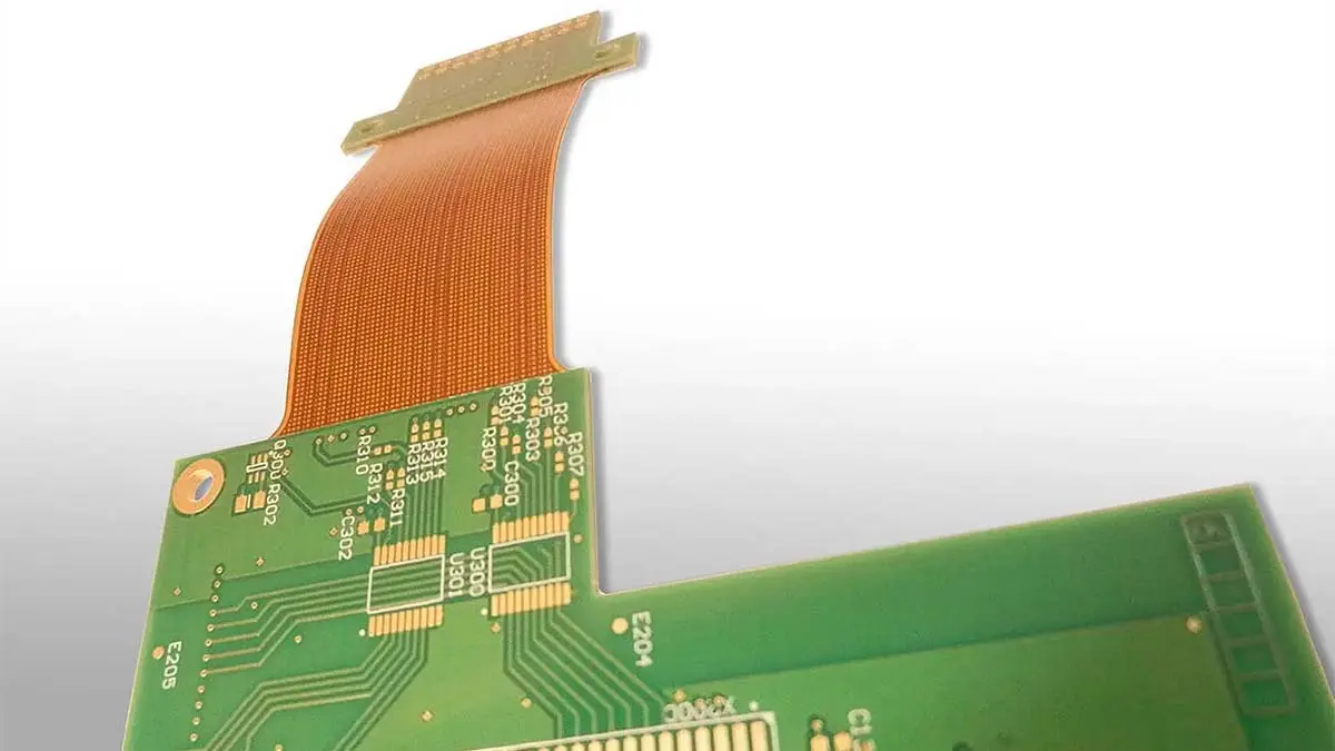
Q3: Can we use a laser depaneling system for flexible PCBs (FPC) used in wearables?
Yes, absolutely. In fact, UV laser is the industry-standard method for separating flex and rigid-flex materials used in wearable medical electronics. It cuts cleanly without tearing, stretching, or delaminating the ultra-thin polyimide films.
Q4: How does a 25μm laser kerf width actually save us money in production?
Standard mechanical routers require a 2.0mm to 3.0mm routing channel to physically pass through the panel. A laser beam only requires a fraction of a millimeter. This allows engineers to nest and squeeze more individual boards onto a single manufacturing panel, directly reducing material waste and substrate costs per unit.
Q5: Is laser depaneling fast enough to keep up with high-volume production lines?
For extremely thick boards requiring long straight cuts, a mechanical saw might have a faster raw cutting speed. However, for high-mix medical production, complex board geometries, or flexible circuits, automated inline laser systems are highly efficient. What you might lose in raw feed-rate speed, you more than make up for by entirely eliminating tool-change downtime, board washing stations, and QA rework.