![]()

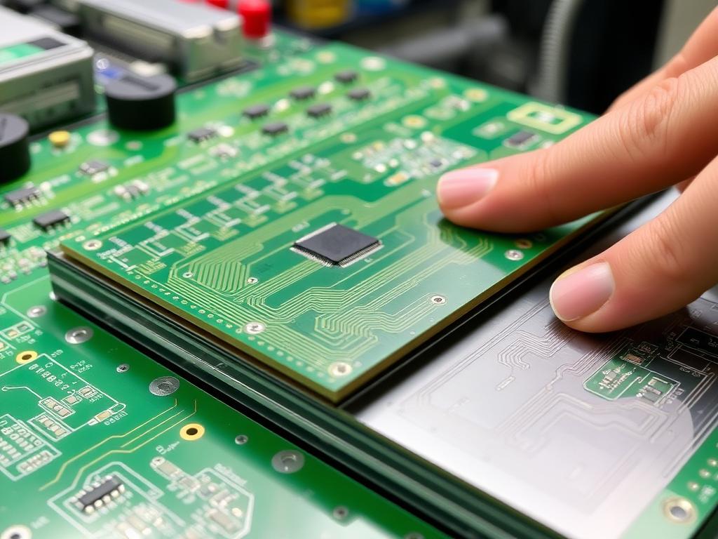
Multi-layer PCB depaneling
Precision PCB Depaneling: Mastering Multilayer PCB Separation for Flawless Circuit Boards
As someone who’s spent the last 20 years deeply immersed in the world of PCB manufacturing, I’ve seen firsthand how critical the depaneling process is. It’s the final step in transforming a large, multi-unit panel into individual, functional circuit boards. In this article, I’ll be sharing my expertise on the different methods of PCB depaneling, with a special focus on the complexities of multilayer pcbs. We will explore various techniques, tools, and best practices to ensure you’re getting the best results for your valuable circuits. Whether you’re a seasoned professional or new to the industry, this guide is packed with insights that can help you optimize your pcb manufacturing process.
What is PCB Depaneling and Why Does It Matter?
PCB depaneling is the process of separating individual pcbs from a larger panel after the pcb manufacturing is complete. Think of it like breaking apart a chocolate bar into individual squares; you start with one big piece and then divide it into smaller pieces, ready to use. This step is crucial because during the pcb fabrication process, it’s much more efficient to produce many circuits on a single plate. Once the electronic components are placed and solder is applied, the larger panel needs to be broken down into those individual pcbs. The precision of this process directly impacts the quality and reliability of the final product. Poor depaneling can lead to mechanical stress, damaging sensitive circuitry and rendering your precious boards useless. For example, excessive force in a manual separation process may lead to small cracks and shorts. We have seen this happen in some of the smaller companies, especially.
We are very meticulous about this stage in the process. As a leader in pcb depaneling solutions, we’ve provided our machines to industry giants like TP-LINK, Canon, BYD, Flex, TCL, Xiaomi, Lenovo, OPPO, HONOR, and Foxconn. These companies rely on precision and efficiency, and we deliver that. We have helped many to achieve consistent separation. These giants require an automated, high-precision solution, which is what our machines are designed to do. We have found that with automation, mechanical stress is greatly reduced.
What are the common depaneling methods used in the industry?
Over my 20 years in this business, I’ve witnessed several methods for pcb depaneling. Each comes with its own set of advantages and disadvantages, depending on the type of pcb being produced. Here are a few common approaches:
- Manual Depaneling: This is the most basic method, using hand tools like a pizza cutter or pliers. It’s suitable for low-volume production or prototyping, but its accuracy is limited, and it often leads to mechanical stress on the board. This method is fine for prototyping and can be considered a good option for very small volumes of production.
- Scoring or V-Groove Depaneling: This involves creating a V-shaped groove along the separation lines of the printed circuit board, allowing the boards to be snapped apart with controlled force. This method is cost-effective and efficient but may not be suitable for all board designs, especially those with components near the edges.
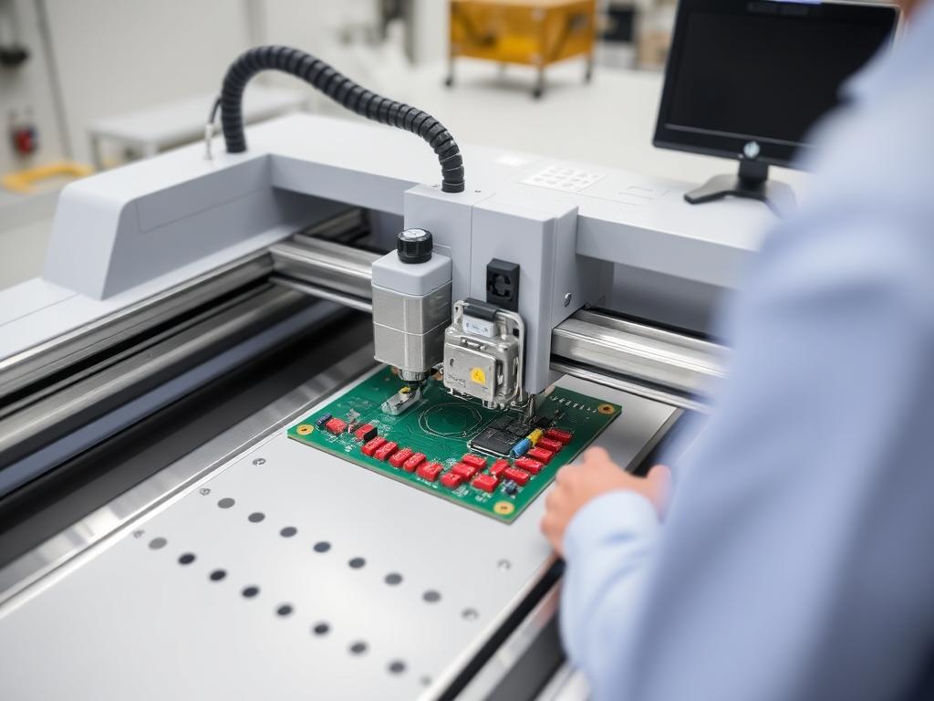
- Routing: This involves using a router to precisely cut along the outline of the pcbs. Routing offers high accuracy, making it suitable for complex shapes and sensitive components. It also leads to a smooth edge quality. We offer a range of router machines for different needs.
- Punching: This method uses a die and press to separate the pcbs. This is a fast option for high-volume production, but it requires custom tooling and is best suited for specific board shapes. It is very precise if you have the correct equipment.
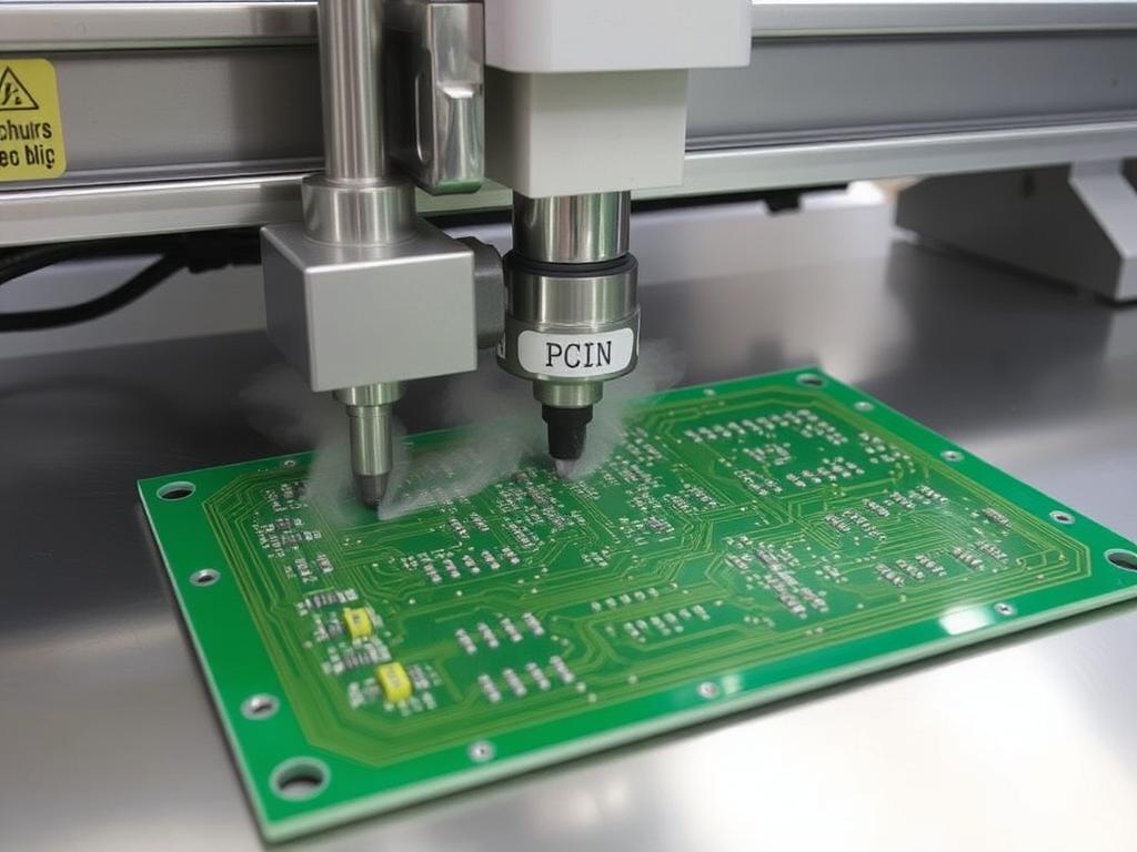
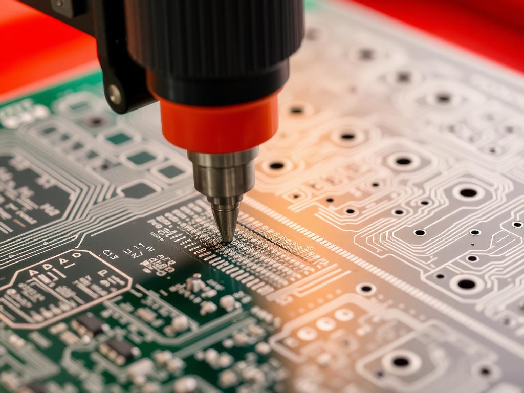
- Laser Depaneling: This is the most advanced method, using a focused laser beam to cut through the printed circuit board. Laser depaneling is highly accurate, minimizes stress, and offers greater design flexibility. We have invested heavily in advanced laser technology to deliver the best results.
Why is laser depaneling gaining popularity?
Laser depaneling has rapidly gained traction in recent years, and for good reason. The ability to use a very thin and precise laser beam to separate the pcbs is revolutionizing the depaneling process. One of the key advantages is its minimal mechanical stress. Unlike other methods that can exert significant pressure on the boards, laser depaneling ensures that the delicate electronic components are not damaged. This is especially vital for multilayer pcbs, where the internal circuitry is more susceptible to damage.
Laser cutting is also highly adaptable. It can easily handle complex shapes and contours that would be difficult or impossible to achieve with other methods. This flexibility is a boon for designers pushing the boundaries of pcb design for electronic devices and smartphones. Furthermore, laser depaneling eliminates the need for tooling, making it ideal for small to medium-sized production runs. This offers pcb manufacturers the flexibility that is needed in today’s market. At PCB Depaneling, we have seen firsthand the benefits our customers get from using our laser depaneling equipment. We believe this is the future of depaneling, and are happy to help customers move into this high-precision method.
How does multilayer PCB depaneling differ from single-layer boards?
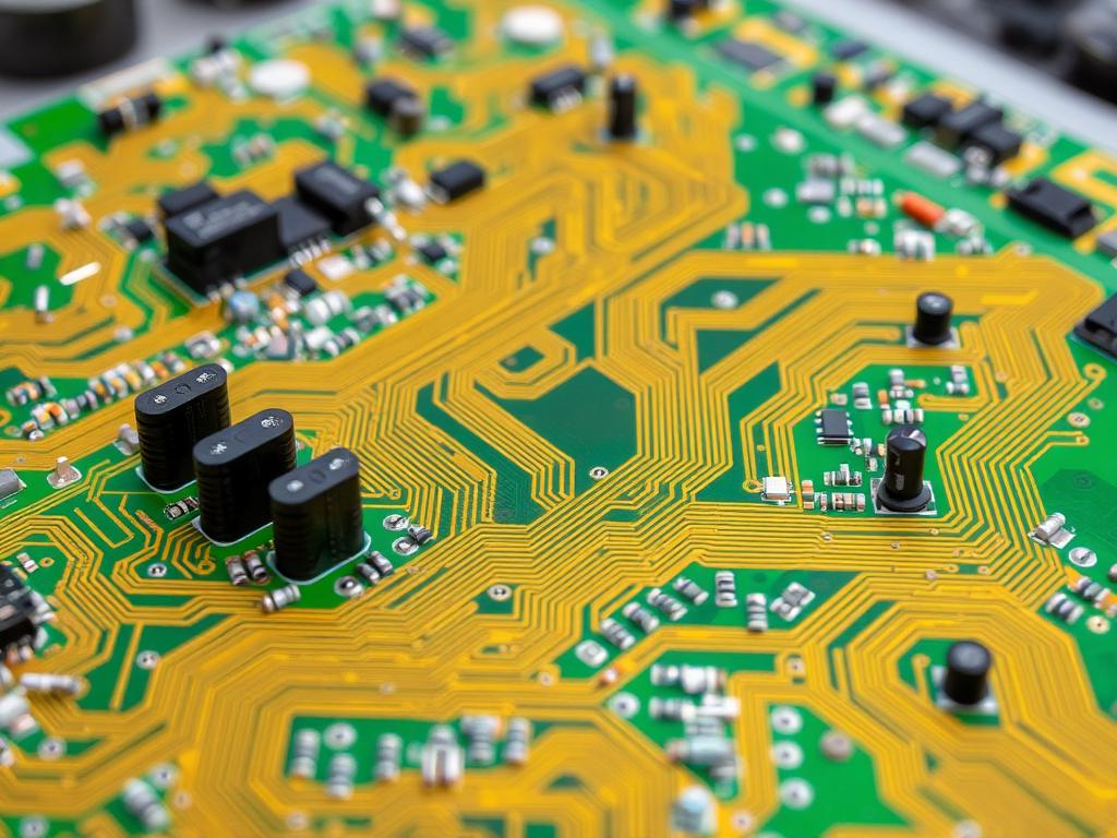
Multilayer pcbs are a marvel of modern engineering. They consist of multiple layers of conductive layers, separated by insulating laminate. These layers allow for more complex circuitry in a smaller form factor. While single-layer boards have connections placed on the top, multilayer printed circuit boards have several copper foil layers with electrical connections formed throughout the board. This complexity also brings challenges, especially when it comes to depaneling. The increased number of inner layers makes these boards more fragile, increasing the risk of damage during separation. This risk is multiplied when using older methods. This fragility makes the separation process a complex procedure.
Standard mechanical depaneling methods can introduce too much mechanical stress, potentially causing delamination, where the layers begin to separate. Therefore, precise methods are essential to maintain the structural integrity and reliability of multilayer boards. Laser depaneling is often the method of choice for multilayer pcbs due to its non-contact nature, which minimizes mechanical stress and reduces the possibility of damage. We have found that the additional cost is justified, as it reduces the number of scrap boards and improves overall reliability of the product.
What are the challenges associated with multilayer pcb manufacturing?
Multilayer pcb manufacturing is a delicate art form. The process involves bonding multiple layers of conductive and insulate materials together, creating a complex stack-up of circuits. The most significant challenge in manufacturing these complex boards is maintaining precise alignment of the layers. Any misalignment can affect the function of the board and lead to defects. The lamination process, during which the layers are bonded together, requires meticulous control of temperature, pressure, and vacuum. Any deviations in these parameters can result in imperfections such as voids and delamination. We have helped to optimize these processes for many of our customers.
Another major challenge is ensuring good signal integrity. In multilayer pcbs, signals can interfere with each other, especially at high frequencies. Careful pcb design and precise fabrication techniques are essential to minimize EMI and signal loss. Moreover, the higher the number of layers, the more complex the manufacturing becomes, leading to longer production times and higher costs. That is why choosing the right depaneling system is very important, as it is critical to the overall success of the manufacturing process. We have spent many years designing solutions to help customers overcome these problems.
What are the different types of PCB depaneling machines available?
Over the years, the advancement of technology has led to the introduction of several types of pcb depaneling machines to meet varied demands and production scales. Here’s a brief look at some of the machines we offer:
- Automatic Router Machines: These machines utilize a high-speed spindle to separate the pcbs by routing along a pre-determined path. They are precise, versatile, and suitable for complex board shapes. Our GAM 330AT In-Line Automatic PCB Router Machine is an excellent example. GAM 330AT In-Line Automatic PCB Router Machine
- Automatic V-Groove Separator: These machines utilize a blade to separate pcbs along a v-groove. They are ideal for high-volume production where the v-groove method is suitable. Our ZM30-ASV Fully Automatic saw-type V-groove PCB depaneling is the right choice for many clients. ZM30-ASV Fully Automatic saw-type V-groove PCB depaneling
- Automatic Laser Depaneling Machines: These machines use a focused laser beam to cut through the material, offering high precision and minimal stress. The DirectLaser H5 is our recommended choice for laser depaneling. DirectLaser H5 PCB-FPC Laser Cutting Machine
- Automatic Punching Machines: These machines use a punch to cut through the material, and are typically faster than milling. We offer the ZM10T & 15T PCB & FPC Punching Cutting Machine for our customers. ZM10T & 15T PCB & FPC Punching Cutting Machine
The right machine will depend on your production volume, board complexity, budget, and required precision. We’ve found that many smaller manufacturers grow with our router and then move into our laser depaneling offerings. We are always available to help our customers find the best solution for their needs.
What is the role of V-groove depaneling?
V-groove depaneling is a common method used in the pcb manufacturing process, particularly for boards that are designed with a predefined snap-off line. During the fabrication stage, a V-shaped cut is made into the laminate material along the edges of the pcbs that need to be separated. The v-groove acts as a guide, allowing the boards to be easily separated through controlled breaking. The biggest advantage of v-groove depaneling is its speed and efficiency. It’s a cost-effective cutting method, which is why it’s widely used for high-volume production of rigid pcbs, such as standard electrical boards. For example, it works well when producing pcbs for consumer electronics.
However, this method in practice has limitations. The quality of the break can vary and may result in some mechanical stress on the board, especially if not performed correctly. It’s not suitable for complex shapes and boards with components that are placed close to the separation line. While v-groove depaneling is not as versatile as laser cutting, it remains a practical solution for many applications where these constraints aren’t an issue. We offer several V-groove depaneling machines, including the ZM30-P PCB Guillotine Separator for high volume applications. ZM30-P PCB Guillotine Separator
How do PCB/FPC punching machines contribute to the separation process?
PCB/FPC punching machines are another efficient solution for pcb depaneling, particularly for high-volume manufacturing. These machines employ a custom-made die and press to cut out the pcbs from the panel. This cutting process is typically faster than routing and can be used with a wide variety of board shapes and sizes. The main benefit of using PCB/FPC punching machines lies in their speed and accuracy. Once the tooling is set up, the separation process is quick and consistent, allowing for large quantities of pcbs to be processed quickly. They’re often used in the production process of smartphones and wearables due to their high throughput capacity.
However, setting up the tooling for each different board design can be time-consuming and expensive. Therefore, these machines are best suited for situations where the volume of pcbs is high enough to justify the initial cost. Another limitation is the type of materials that can be processed. Thicker pcbs may require more powerful machines and special tooling. Despite these limitations, our customers see tremendous benefits in the right environment. The ZM10T & 15T PCB & FPC Punching Cutting Machine is a versatile option. ZM10T & 15T PCB & FPC Punching Cutting Machine
Why is precision so important when depaneling circuits?
Precision in depaneling is paramount, especially with the increased use of multilayer pcbs and miniaturized electronic components. Inaccurate depaneling can cause various issues that can compromise the reliability and performance of the final product. Damage to delicate surface-mount electronic components and through-holes are some of the common issues related to the cutting process. Incorrect cutting method can cause stress fractures in the laminate material, leading to premature failure. This is especially important in critical applications such as medical devices and aerospace equipment.
Another often overlooked issue is the risk of delamination in multilayer pcbs. Incorrect separation can cause the layers to separate, causing damage to the circuitry within. When it comes to multilayer printed circuit boards, maintaining precision is vital, as these boards have layers and more complexity compared to double-layer pcbs. Precise separation eliminates the need for subsequent cleaning, thus reducing manufacturing costs and ensuring high-quality individual printed circuit boards. This is why we put so much focus on high precision technology. When you purchase our pcb depaneling machinery, we provide the best result.
How do I choose the right depaneling method for my pcbs?
Choosing the right depaneling method depends on many factors, including the type of pcb, production volume, budget, and the complexity of the design. Here’s a simple guide to help you make an informed decision:
- For prototyping and low-volume production: Manual methods like scoring or hand tools may suffice if you don’t need a large number of pcbs. However, keep in mind that this can be inefficient.
- For medium-volume production of simple boards: V-groove depaneling may be suitable if the design allows.
- For complex shapes and designs: Routing offers versatility and precision.
- For high-volume production with regular shapes: Punching is a fast and efficient option, provided that the number of pcbs is large enough.
- For high-precision and sensitive applications (especially multilayer pcbs): Laser depaneling is the ideal choice due to minimal mechanical stress and high adaptability.
We at PCB Depaneling, with our 20 years of experience, understand that there is no one-size-fits-all solution, and will help to analyze your specific needs to recommend the best solution. Contact us today to discuss your needs, and let us be your guide.
FAQs:
What is the difference between routing and laser depaneling? Routing uses a rotating tool to cut the pcb, while laser depaneling uses a focused laser beam. The laser method is more precise, and reduces mechanical stress. We have seen that it is preferred in advanced manufacturing.
Can laser depaneling be used for all types of PCBs? Laser depaneling can be used on a wide range of materials, but it is particularly advantageous for multilayer pcbs and those with intricate designs, because of reduced stress and high precision.
How can I reduce mechanical stress during depaneling? The best way to minimize mechanical stress is to use precise depaneling methods such as laser cutting or high-quality routing machines. Proper maintenance of the depaneling system can also play a part.
What are the key considerations for multilayer PCB depaneling? When dealing with multilayer pcbs, it is important to choose a method that minimizes stress on the board. Laser depaneling is often favored due to its non-contact approach, which reduces the risk of delamination and damage.
What level of production volume is appropriate for a punching machine? Punching is ideal for high-volume productions because the setup cost and time are higher than laser and router machines. It’s crucial that you have enough throughput to justify the initial investment.
- Summary:
- PCB depaneling is a vital part of the pcb manufacturing process, separating individual pcbs from a panel consisting of multiple layers.
- There are different depaneling methods, including manual, v-groove, routing, punching, and laser depaneling.
- Laser depaneling is gaining popularity due to its precision, minimal mechanical stress, and versatility with different types of pcbs.
- Multilayer pcbs require extra caution during depaneling due to their complex structure and sensitivity to damage, and require a high level of precision and advanced techniques.
- Choosing the right depaneling method depends on several factors, such as complexity of the design, and production volume.
- Our 20 years of expertise have made us a leader in pcb depaneling, trusted by leading companies such as TP-LINK, Canon, BYD, Flex, TCL, Xiaomi, Lenovo, OPPO, HONOR, and Foxconn.
- Contact us today to discuss your pcb depaneling needs and let us provide you with an optimized solution.