![]()
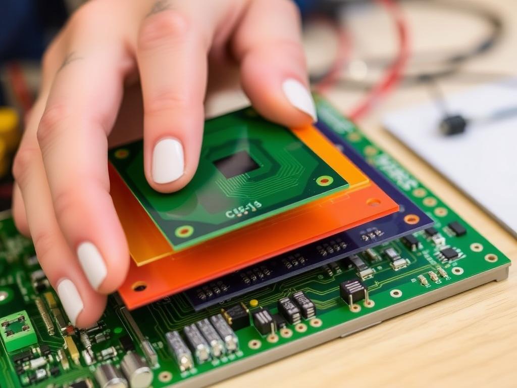
how to separate pcb layers
Mastering PCB Layer Design: A Comprehensive Guide to Multi-Layer PCB Manufacturing
In today’s fast-paced electronics manufacturing world, understanding PCB layer design is crucial for producing high-quality circuit boards. Whether you’re working on simple two-layer boards or complex multilayer PCBs, proper layer management can make the difference between success and failure. This guide will help you navigate the complexities of PCB layer design while highlighting modern manufacturing solutions.
What Makes Multi-Layer PCB Design So Important?
The evolution of electronic devices has driven the need for increasingly complex PCB designs. Modern multilayer PCBs allow for:
- Higher component density
- Better signal integrity
- Improved electromagnetic shielding
- Enhanced power distribution
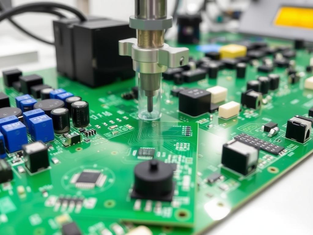
Our GAM330AD In-Line Automatic PCBA Router Machine helps achieve precise layer separation during manufacturing.
Understanding PCB Layer Stack-Up
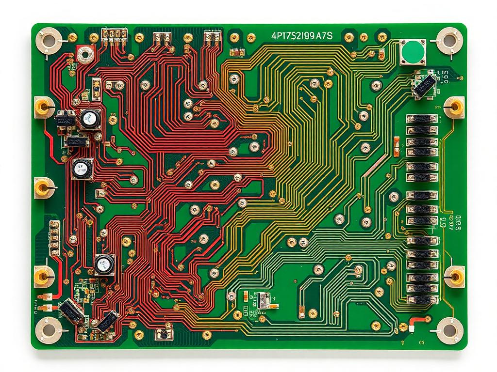
A proper PCB layer stack-up is fundamental to successful board design. Here’s what you need to know:Common Layer Configurations:
| Layer Count | Typical Use | Complexity Level |
|---|---|---|
| 2 Layer | Simple devices | Basic |
| 4 Layer | Consumer electronics | Intermediate |
| 6+ Layer | High-performance devices | Advanced |
How Does Layer Splitting Affect Signal Integrity?
Signal integrity is critically dependent on proper layer management. Consider these factors:
- Return path planning
- Power plane distribution
- Ground plane continuity
Explore our V-Groove Depaneling solutions for precise board separation.
Power and Ground Plane Considerations
Effective power distribution requires careful planning:
- Dedicated power planes
- Strategic via placement
- Proper decoupling capacitor placement
Advanced PCB Layout Techniques
Modern PCB design demands sophisticated approaches:
- Controlled Impedance Routing
- Trace width calculation
- Layer spacing optimization
- Material selection
- EMI Mitigation
- Shield layers
- Ground plane design
- Component placement
Check out our PCB/FPC Punching Machine solutions for precise manufacturing.
FR4 Material Properties and Layer Considerations
FR4 remains the most common PCB substrate material. Key considerations include:
- Dielectric constant
- Loss tangent
- Thermal properties
Manufacturing Challenges in Multi-Layer PCBs
Common challenges include:
- Layer alignment
- Copper thickness consistency
- Via aspect ratios
Our Automatic Equipment solutions help overcome these challenges.
Frequently Asked Questions
How many layers should my PCB design have?
The number of layers depends on your application’s complexity, signal integrity requirements, and cost constraints. Most designs range from 2 to 12 layers.
What’s the minimum spacing between layers?
Typical minimum spacing is 0.004″ (0.1mm), but this varies based on manufacturer capabilities and design requirements.
How do I prevent signal interference between layers?
Use ground planes between signal layers, maintain proper stackup design, and implement proper routing techniques.
What’s the maximum number of layers possible in a PCB?
While theoretically unlimited, practical manufacturing limitations typically cap at 32 layers for most applications.
Best Practices for Layer Management
- Documentation
- Clear layer stackup diagrams
- Detailed manufacturing notes
- Comprehensive design rules
- Quality Control
- Regular testing procedures
- Impedance verification
- Layer alignment checks
Discover our SMT whole line equipment for complete manufacturing solutions.
Key Takeaways
• Proper layer stack-up is crucial for PCB performance • Material selection impacts overall board quality • Manufacturing processes must be considered during design • Quality control is essential throughout production • Professional equipment ensures precise manufacturing • Regular testing and validation ensure maintained performanceContact us to learn how our advanced PCB manufacturing solutions can optimize your production process.
