![]()

PCB-Depaneling für tragbare Geräte
From Manual to Laser: A Deep Dive into PCB Depaneling Methods
As someone with over 20 years immersed in the Leiterplatte industry, I’ve seen firsthand the incredible evolution of Leiterplatten-Nutzentrennung. From rudimentary manual methods to the precision of Laser-Nutzentrennen, the way we separate individual Leiterplatten has dramatically changed. This article isn’t just a technical overview; it’s a journey through the different approaches, highlighting the pros, cons, and why choosing the right method is crucial for efficient and high-quality Leiterplattenherstellung. Whether you’re a seasoned engineer or a Leiterplatte enthusiast, understanding these nuances is key to producing top-notch electronic products. Let’s explore the world of Leiterplatten-Nutzentrennung together.
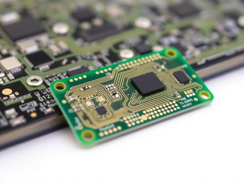
What Exactly is PCB Depaneling and Why Is It Necessary?
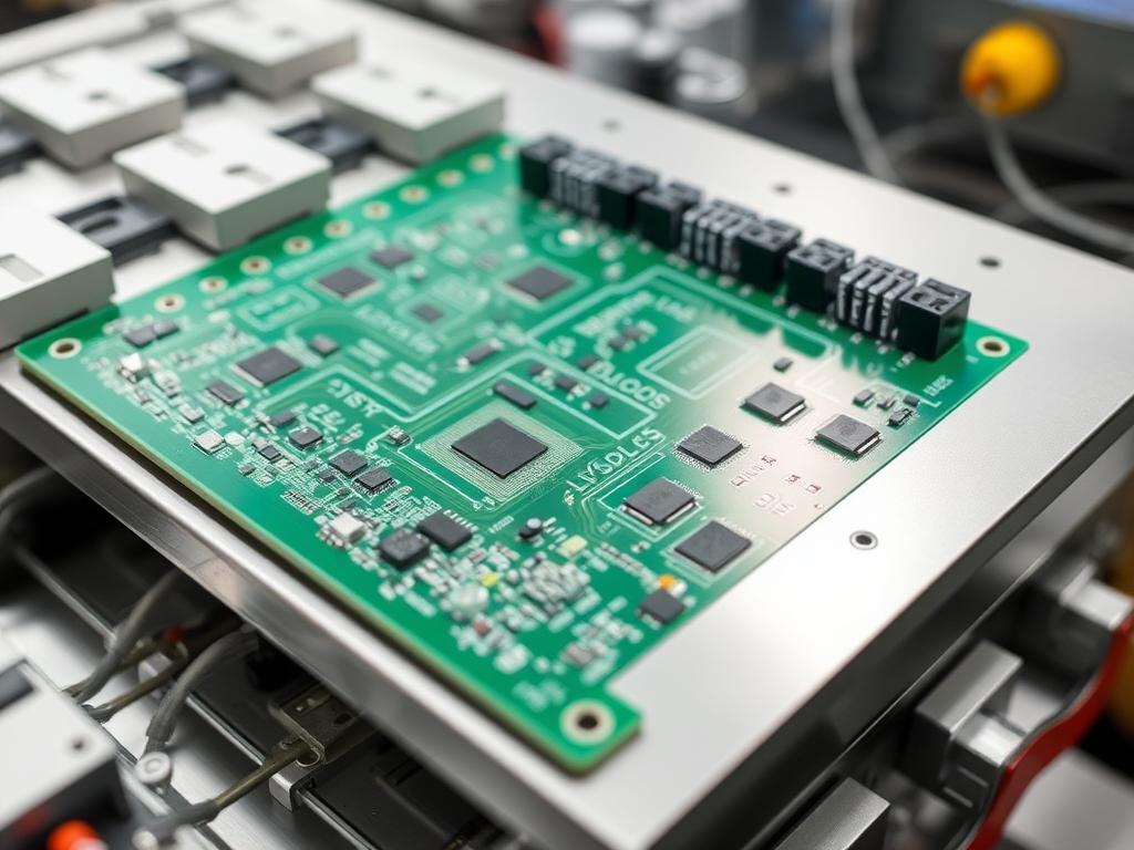
As someone who has seen countless Leiterplatten go from large panels to individual Leiterplatten, I can tell you that Leiterplatten-Nutzentrennung is an absolutely critical step in the Herstellungsverfahren. Imagine a sheet of connected Leiterplatten – that’s how they’re created in order to maximize efficiency. Nutzentrennen ist das Prozess der Entfernung those individual Leiterplatte from the larger panel after all the components have been placed and Lot has been applied, ready for use in elektronische Geräte. This stage, sometimes also called singulation, is when we carefully separate the individual Schaltkreise.
The purpose of this process is simple: to transform a large, unwieldy panel of Leiterplatten in die einzelnen Leiterplatten that are essential for all kinds of electronic applications. These Leiterplatten are then ready to be integrated into various electronic assemblies. Without Nutzentrennen, we wouldn’t have the individual, functional boards needed for everything from smartphones to industrial equipment. As these pcbs are typically produced on a larger panel, Nutzentrennen is what makes each one a standalone product.
What are the Different Depaneling Methods Used in PCB Manufacturing?
Over the years, I’ve used and seen several Methoden zum Leiterplatten-Nutzentrennen in action. From the older techniques to state-of-the-art methods, each has its own strengths and weaknesses. In the early days, we relied on manual methods, which involved physically breaking apart the Leiterplatten. While this was simple, it was also time-consuming and prone to errors. Then came the introduction of Stempel tooling, where a tool is used to create a separation through a specific die, creating a more uniform separation.
However, the real advancements came with the use of automated machinery. We started using router cutting, which employed a spinning tool used to cut along the designated separation line. This technique provided much better accuracy and efficiency compared to manual methods. Now, Laser-Nutzentrennen is becoming increasingly popular due to its precision and ability to cut complex shapes, and Laserfräsen is rapidly becoming the most used Schneideverfahren. Each of these Trennverfahren is still used today, and the choice depends on factors such as the type of Leiterplatte, desired precision, and Durchsatz Anforderungen.
How Does Router Cutting Compare to Other PCB Depaneling Techniques?
As someone who’s worked with both Router cutting and other techniques, I’ve seen the pros and cons firsthand. Router cutting, a method I’ve used extensively, involves a spinning bit that precisely separates individual printed Leiterplatten. It’s a workhorse in the industry, offering a balance of speed and accuracy. However, it’s not perfect for every situation.
Einer der Hauptvorteile von Router cutting is its ability to handle various Substrat materials and thicknesses. It’s reliable and has a relatively low cost of operation, making it a go-to for many Leiterplattenbestückung plants. However, there are downsides. Router cutting introduces mechanische Beanspruchung zur Leiterplatten, which can be a problem for sensitive components, particularly around the Lötstellen. This stress may also lead to micro-cracks or warping, especially on very thin Leiterplatten. Additionally, the Schnittbreite, or the amount of material removed by the cutting bit, can sometimes be quite large. This can limit how closely we can pack Leiterplatten together on a panel, which increases waste. Comparing this to Laser-Nutzentrennen, Die Router technique is less precise, and introduces more stress.
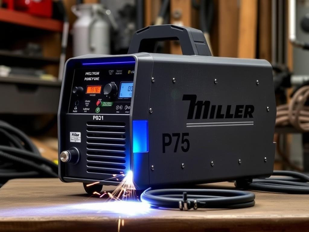
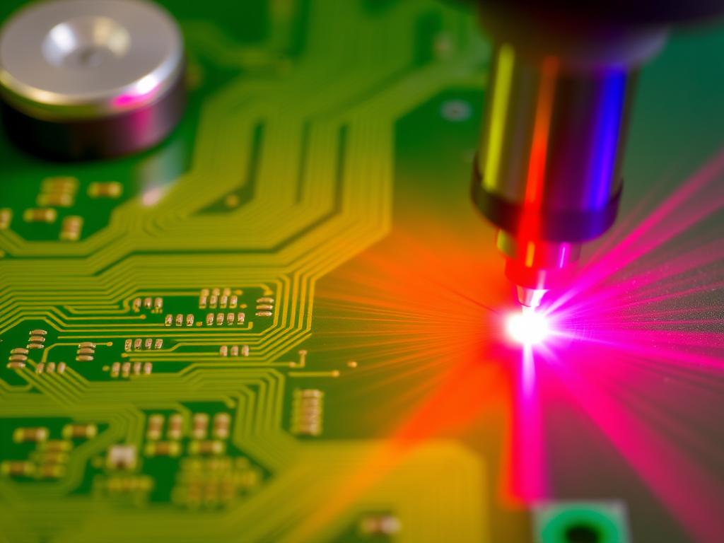
What is Laser Depaneling and How Does it Work?
Laser-Nutzentrennen has always fascinated me, even after years of working in the Leiterplatte industry. It is a cutting system that has really changed the industry, using a focused Laserquelle trennen individual circuits from the larger panel. Unlike mechanical cutting systems such as a Router, Laserschneiden is a non-contact process, which greatly reduces the mechanische Beanspruchung und die part induced stress auf der Leiterplatten. This is particularly beneficial for sensitive components and high-density layouts.
The process involves directing a UV-Laser beam with extremely high energy density onto the Leiterplatte. Der Laser vaporizes the material along the Schnittlinie, creating a very narrow Schnittbreite compared to traditional methods. The precision of the Laser-Nutzentrennen is extraordinary. It is possible to create very fine and intricate cuts and allows for complex shapes that cannot be achieved with a Router, for instance. This method is great for intricate designs and especially beneficial when working with biegen Und rigid flex pcbs, which are more susceptible to mechanical damage. However, one drawback of Laser-Nutzentrennen is that it’s typically a slower process than Router cutting, which can lead to lower Durchsatz.
How is Laser Routing Revolutionizing the PCB Industry?
The introduction of Laserfräsen has been transformative in the Leiterplattenfertigungsindustrie. It represents a significant step in the evolution of pcb depaneling and continues to impact all aspects of our work. It’s not just about cutting; it’s about precision, flexibility, and the ability to handle increasingly complex Leiterplatten.
Laser routing offers several significant advantages compared to traditional methods. First and foremost, its precision is unparalleled, with minimal Schnittfuge, and it minimizes the risk of damage. This is particularly important when working with biegen Und rigid flex pcbs, which are often used in wearables and other sensitive applications. The non-contact nature of the Laser means there’s no risk of stressing the delicate components and the extremely precise Fokussierte Spotgröße ensures clean and accurate cuts, vital for the smaller components we use today. I’ve personally witnessed how Laserfräsen has enabled us to produce incredibly complex board shapes and features that simply weren’t possible with traditional methods, making it an essential technology for advanced electronics. It is also far more flexible than Router oder Stempel, as the Laser can be used to cut along any designed Schnittlinie, meaning new designs are easy to implement.
What Role Does Flex PCB Depaneling Play in Wearable Technology?
As someone deeply involved in the manufacturing process of flexible printed circuits, I’ve seen firsthand how crucial flex pcb depaneling plays, especially in the booming market of wearable Technologie. Flex pcbs Und rigid flex pcbs are the cornerstone of many wearables and other applications that require miniaturization and flexibility. These thin and flexible circuit boards enable designers to create devices that conform to different shapes and offer greater freedom in the mechanical design of elektronische Geräte.
Flex pcb depaneling plays a pivotal role in the manufacturing process of these flexible Leiterplatten. Wearable devices, such as smartwatches, fitness trackers, and other wearables, all rely on these flexible Leiterplatten. Der process of flexible printed circuit board separation is particularly challenging because the biegen materials are extremely sensitive to stress, and flex pcbs are even more susceptible to damage than rigid Leiterplatten. Laser-Nutzentrennen wird oft bevorzugt für flexible Leiterplatte separation due to its non-contact nature and precision. This method ensures that the Leiterplatten are cleanly separated without introducing the mechanische Beanspruchung or damage that may result in damage of the components or Lötstellen.
What is the future for PCB Depaneling systems?
Die Zukunft von Leiterplatten-Nutzentrennung is about automation, flexibility, and even greater precision, as I have seen the technology evolve over the years. The trend is towards creating more efficient, versatile, and intelligent Nutzentrennsysteme. We are likely to see even more integration of Laserfräsen technology, not just due to it’s greater precision, but also due to its flexibility for working with new designs. As Leiterplatten become smaller and more complex, the need for precision laser pcb depaneling systems will grow significantly.
Beyond the Laserquelle, automation is becoming key. This not only speeds up the Nutzentrennungsprozess and reduces labor costs, but it also improves consistency and reliability. The Leiterplatten-Nutzentrennung field will become more advanced, with Nutzentrennsysteme integrating real-time monitoring and feedback systems to ensure quality, and adaptive systems that can adjust to variations in materials and designs automatically, minimizing waste and optimizing Durchsatz. The future of Leiterplatten-Nutzentrennung is a symphony of high-precision machines and intelligent control systems.
Why is precision so critical in the Depaneling Process?
In the world of Leiterplattenherstellung, precision is not just a nice-to-have; it’s an absolute necessity. The Nutzentrennungsprozess is the last step before these individual printed Leiterplatten are integrated into devices, and if this step is not done precisely, it can lead to problems down the line. I’ve seen firsthand how even small errors in Nutzentrennen can result in faulty products, delays, and additional costs.
The need for accuracy in Nutzentrennen stems from the delicate nature of modern Leiterplatten. Diese Leiterplatten are densely packed with small components, and any unnecessary mechanische Beanspruchung, or deviations in the Schnittlinie, can cause damage. Issues can range from micro-cracks in the Substrat to damage to Lot joints or the components themselves. The use of precise techniques, like Laserfräsen, ensure that the Leiterplatten are separated cleanly, minimizing the risk of defects. This level of precision ultimately contributes to higher quality products and greater reliability of the elektronische Geräte.
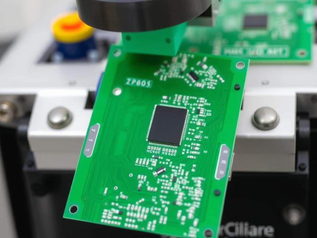
What are the key components of an automated PCB depaneling system?
Having worked with automated Nutzentrennsysteme for years, I’ve come to appreciate the importance of each component and how they all work together to ensure high-quality Leiterplatte separation. These complex systems are the backbone of efficient Leiterplattenherstellung, and several key components are crucial for proper operation.
The most fundamental component of any automated system is the handling system that move the Leiterplatten from the in-feed to the out-feed. This system ensures the correct positioning for the cutting systems, whether it is a Router oder ein Laser. The vision system, incorporating cameras and sophisticated software, allows for precise alignment of the Schnittlinie, ensuring consistency and accuracy. Another critical component is the control system, which manages the entire operation. This includes the computer controls, and the interface which can allow operators to monitor progress and make adjustments as needed. In a Laser-Leiterplatten-Nutzentrennung system, the Laserquelle itself is a critical component, responsible for the precise separation of the Leiterplatten.
Final Thoughts on Choosing the Right Cutting Systems
Throughout my career in the pcb manufacturing industry, I’ve learned that choosing the right cutting systems für Nutzentrennen is crucial. The process is not just about separating Leiterplatten; it’s about efficiency, precision, and minimizing waste. We’ve gone from manually breaking Leiterplatten apart to using sophisticated machinery, so the correct choice of Depaneling-Verfahren depends on the specific requirements of your product.
For example, if you’re working with flex pcbs or high-density layouts, you might be better served by the precision and low-stress nature of Laser-Nutzentrennen oder Laserfräsen. However, if you’re dealing with less sensitive designs and lower volumes, Router cutting might be a cost-effective option. The key is to evaluate all your needs: the complexity of the Leiterplatte, the required Durchsatz, and sensitivity to mechanische Beanspruchung, and so on. This will ensure that you choose the best possible Schneideverfahren für Ihren spezifischen Anwendungszweck.
Remember, the goal of Nutzentrennen is to produce high-quality Leiterplatten that meet all specifications and requirements. As the technology continues to advance, I’m confident that the future of Nutzentrennen will lead to ever greater levels of efficiency and precision. At PCB-Nutzentrennung, we are dedicated to providing the best technology for your business, from PCB-Fräsmaschinen, Zu V-Nut-Nuttrennung, Und PCB-Laser-Nutzentrennen systems. We offer solutions from manual to laser, and we can advise you on the best method to suit your manufacturing requirements. Don’t hesitate to contact our sales team for a quote, or if you require assistance with Leiterplatten-Nutzentrennung.
- To see the full range of our PCB-Fräsmaschine, visit our Produktseite.
- If you would like to know more about V-Nut-Nuttrennung, we have a complete list of products Hier.
- For those interested in the latest in PCB-Laser-Nutzentrennen see our page
- You may be interested in our PCB/FPC-Stanzmaschine solutions that we offer Hier.
- To see our entire range of Automatische Ausrüstung, please click Hier
- And for a complete list of Zubehör, see our page.
FAQs
How can I minimize stress on my Leiterplatten während Nutzentrennen? Choosing a non-contact method such as Laser-Nutzentrennen is the most effective way to minimieren stress on your Leiterplatten während der Nutzentrennen Verfahren. Laser routing avoids the mechanische Beanspruchung Das Router Und Stempel methods can impose.
What is the best Schneideverfahren für flex pcbs? Laser-Nutzentrennen is generally considered the best method for flex pcbs Und rigid flex pcbs. Its precision and minimal mechanische Beanspruchung ensures that delicate boards are separated cleanly and without damage.
What’s the difference between Router cutting and Laserfräsen? Router cutting uses a spinning bit to separate Leiterplatten, which creates mechanische Beanspruchung, and produces a wider Schnittbreite. Laser routing, on the other hand, uses a focused Laser beam. It is a non-contact process, which eliminates mechanische Beanspruchung and provides much more accurate cuts with a narrower Schnittbreite.
What factors should I consider when choosing a Nutzentrenner? When choosing a Nutzentrenner, consider factors such as the types of Leiterplatten you’re working with, desired precision, Durchsatz, Schnittfuge, and the level of automation you require.
Can you integrate the Nutzentrennsysteme into a full production line? Yes, all the Nutzentrennsysteme that we supply can be integrated into a full production line, with full automation. We offer solutions for in-line SMT production, and many other options. See our SMT-Komplettanlagen Seite für weitere Details.
Zusammenfassung
- Leiterplatten-Nutzentrennung is essential for separating individual Leiterplatten from larger panels, and is a critical step in the Herstellungsverfahren.
- Anders Trennverfahren exist, including manual, Stempel, Router cutting, and Laser-Nutzentrennen, each with its own pros and cons.
- Router cutting is a common method but can induce mechanische Beanspruchung and is not suitable for all designs.
- Laser-Nutzentrennen provides unmatched precision and minimizes stress, making it ideal for flex pcbs, Und rigid flex pcbs, along with complex designs.
- Laser routing is revolutionizing the industry with its high precision and ability to cut complex shapes.
- Flex pcb depaneling is vital for the Herstellungsverfahren von wearable technologies, and other applications that require flexible boards.
- Die Zukunft von Nutzentrennen involves greater automation, precision, and real-time monitoring.
- Die Wahl des richtigen Nutzentrenner depends on the specific requirements of the Leiterplatte design and application.
- Precision is key to ensure the high quality of the final product and avoiding any damage during the Prozess der Entfernung Die individual circuits.