![]()

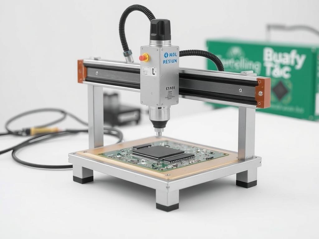
FPC depaneling machine
Precision PCB Depaneling: Mastering the Art of Circuit Separation for Flex, Rigid, and Laser Applications
For over two decades, I’ve been immersed in the intricate world of Leiterplattenherstellung, witnessing firsthand the evolution of Nutzentrennen techniques. The journey from individual Leiterplatten on a large panel to separate, functional units is a critical one, and it’s where precision and efficiency truly matter. This article delves into the crucial process of Leiterplatten-Nutzentrennung, exploring the different methods available, especially focusing on Laser-Nutzentrennen, and why choosing the right solution can make or break your production goals. If you’re involved in Leiterplattenherstellung and looking to optimize your processes, this is a must-read. Whether you are dealing with rigid Leiterplatten, flexible pcbs, or the increasingly popular flex pcbs, understanding the nuances of Nutzentrennen is paramount. We’ll explore how advancements in technology, like Lasertechnologie, have changed the game.
1. What is PCB Depaneling and Why is it so Critical?
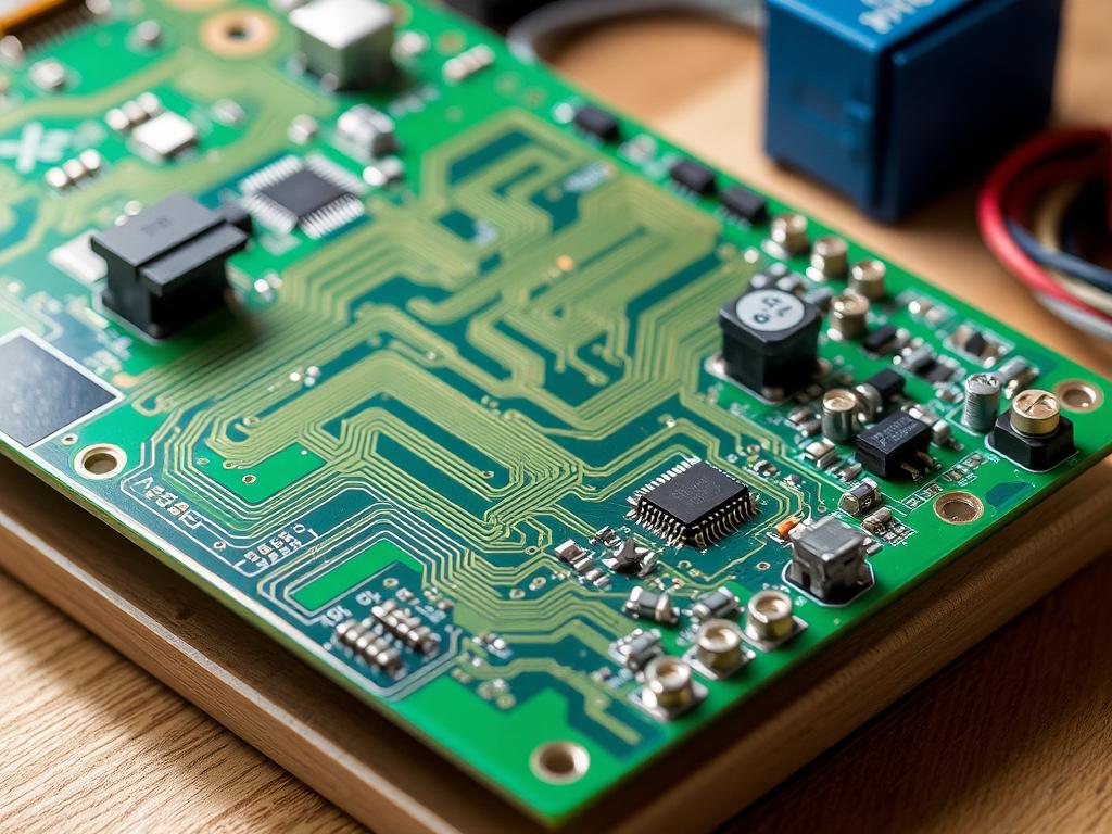
In the world of Leiterplattenherstellung, Leiterplatten are typically produced in large panels containing multiple boards. This approach is cost effective and allows for efficient handling during the Leiterplattenbestückung process. But these individual Leiterplatten must be separated before they become part of their respective elektronische Geräte, and that’s where Nutzentrennen comes in. Nutzentrennen, also called Vereinzelung, is the Prozess der Entfernung Person Leiterplatten from the larger panel. This Trennverfahren requires precision to ensure that the Schaltung isn’t damaged and that the final product functions perfectly. Think of it like carefully cutting out shapes from a sheet of paper—you need the right tools and technique for a clean result. Incorrect Nutzentrennen kann führen zu mechanische Beanspruchung auf der Leiterplatte, potentially causing damage to components and traces, and ultimately leading to failure of the final product. The Nutzentrennungsprozess is therefore a crucial step that bridges the gap between efficient panel production and functional end products.
The role of Nutzentrennen is vital. It directly impacts the quality and reliability of the final Leiterplatte. From my 20 years of experience, I’ve seen that selecting the right Nutzentrennen method not only ensures that the individual Leiterplatten are separated without any problems, but it also contributes significantly to overall efficiency. Improper techniques can lead to several issues, such as cut edge burrs, micro-cracks, and even damage to the delicate leitfähig traces. These defects can have devastating effects on the performance of the assembled devices and can drastically increase production costs due to rework and scrapped parts. The importance of precise and reliable Nutzentrennen cannot be overstated, making it a critical area for continuous improvement and innovation within the Leiterplattenherstellung Verfahren.
2. What are the Main Depaneling Methods for Circuit Boards?
Over the years, I’ve seen a variety of Trennverfahren come and go, each with its own strengths and weaknesses. Among the most common pcb depaneling methods are:
- V-Nut-Nuttrennung: This involves using a V-Schnitt auf der Leiterplatte panel. Then the panel is broken along these lines. This is a cost-effective approach but is suitable only for straight lines.
- Fräsen: A Router is used to cut along the separation line. This is a versatile method suitable for various shapes. It is known for its flexibility. Router cutting does create more dust and requires a Vorrichtung to hold the board in place.
- Stanz-Nutzentrennung: A Stempel and die are used to stamp out individual boards. This is fast but is only suitable for simple shapes and requires expensive tooling.
- Laser-Nutzentrennen: Utilizing Lasertechnologie zum präzisen Schneiden der Leiterplatte, this method offers high precision, minimal mechanische Beanspruchung, and can handle complex shapes. It’s a more recent advancement, and one that I believe is the future of Nutzentrennen, particularly for flexible pcbs.
Each method comes with its own set of advantages and disadvantages. The choice of the Schneideverfahren depends on various factors, including the type of pcb materials used, the complexity of the board shape, and the required Durchsatz. Zum Beispiel, rigid pcbs, particularly those made of fr4 with basic shapes, can be separated using V-Schnitt or even die cutting methods. However, for intricate designs and materials, such as flexible Leiterplatten made of Polyimid, Laser-Nutzentrennen emerges as the preferred choice due to its unmatched precision and minimal impact. As technology advances, the need for more precise and versatile methods is driving innovation in Nutzentrennen.
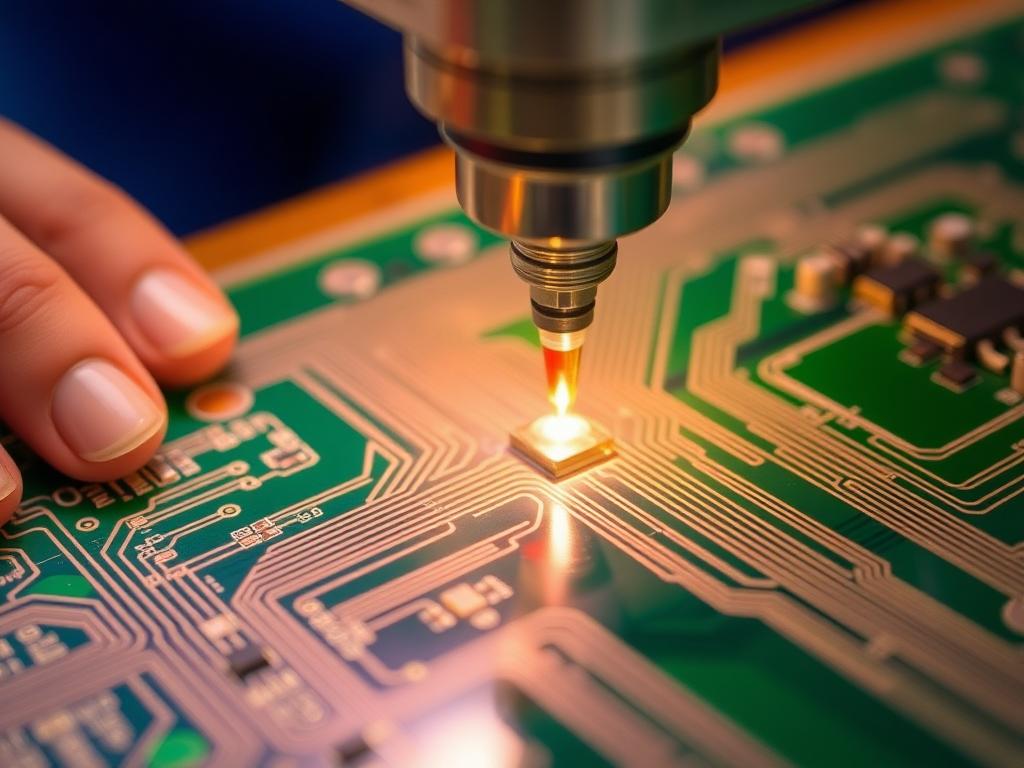
3. Why is Laser Depaneling Gaining Popularity?
In my opinion, Laser-Nutzentrennen represents a monumental leap forward in Leiterplatten-Nutzentrennung. The main reason for its increasing popularity is its unparalleled precision. Unlike mechanical methods that can exert mechanische Beanspruchung auf der Leiterplatte and cause damage, Laser-Nutzentrennen verwendet einen fokussierten Lichtstrahl zum Verdampfen der Substrat, resulting in a clean, precise cut edge without physical contact. This is particularly important when dealing with delicate flexible Leiterplatten that require a very precise and minimal impact approach. Furthermore, the Laser can handle complex shapes and intricate cuts, something that other methods struggle to achieve.
Laser-Nutzentrennen also allows for greater flexibility in terms of material processing. Whether you’re working with fr4, Polyimid, or other pcb materials, Die Laser can be adjusted to suit the specific requirements of each material. This adaptability means that a single Laser-Nutzentrennungssystem can be used for a range of different Leiterplatte types, reducing the need for multiple Nutzentrenner and streamlining the Herstellungsverfahren. For instance, I’ve seen that many of our customers who have switched to Laser-Nutzentrennen have seen a significant increase in both precision and efficiency, as well as reduced material waste. From experience, I can confirm the advantages of the laser, this advanced Schneiden method leads to less post-processing and improved quality, especially in high-precision applications. The laser depaneling process has truly reshaped the approach to the Trennverfahren in modernen Leiterplattenherstellung.
4. What are the Advantages of Using Flexible PCBs in Electronic Devices?
Der advent of new technologies has dramatically transformed the field of electronics, and flexible Leiterplatten have emerged as a game-changer. Flexible printed circuit oder flexible Leiterplatte, made of materials such as Polyimid, offer a host of advantages over traditional rigid pcbs. I’ve witnessed the rise of flexible pcbs across a broad range of products due to their unique characteristics and capabilities. One of the main advantages of flexible boards is their ability to conform to almost any shape. They can be bent, folded, and twisted without compromising their electrical functionality, allowing for innovative designs and compact solutions in elektronische Geräte. They are also lighter and thinner, making them ideal for applications where space and weight are critical.
Flexible Leiterplatten have revolutionized the way we approach the design and manufacturing of elektronische Geräte. They play a vital role in the manufacturing process of many consumer electronics, including smartphones, wearable technology, Und Automobilindustrie applications. The ability of flexible Leiterplatten to accommodate dynamic flexing and vibration makes them incredibly robust and reliable, and this is why they have found widespread use in demanding applications. From my experience, flexible pcbs offer a much greater level of design freedom compared to rigid pcbs, making it possible to create products that are not only functional but also aesthetically pleasing and ergonomic. These characteristics have fueled the growth of flex pcbs and their adoption across diverse industries. The process of flexible board production has become increasingly efficient, and the versatility they offer is unmatched.
5. How does Laser Cutting impact Flexible PCBs?
Wenn es darum geht flexible pcbs, Laserschneiden ist das Schneideverfahren of choice for high precision and minimal mechanische Beanspruchung. Traditional mechanical Leiterplattenschneiden methods often exert pressure on the delicate Substrat, which can lead to damage or deformation of the flexible Leiterplatte. However, a Laser, like a fine surgical tool, precisely cuts without any physical contact, therefore Laserschneiden is an ideal solution for processing these delicate flexible Leiterplatten.
The impact of Lasertechnologie An flexible pcbs is truly transformative. The Laser provides incredible precision. The laser depaneling process stellt sicher, dass die cut edge is exceptionally clean, with no burrs or debris that might compromise the performance of the finished Schaltung. The ability of the Laser to handle intricate shapes and complex layouts is crucial for the design freedom that flexible pcbs offer. When comparing it to other Trennverfahren, I’ve found that Laserschneiden not only reduces the risk of damage but also improves the overall quality and reliability of the Leiterplatten. This results in better performance and longer lifespan of elektronische GeräteDie Verwendung von UV-Laser technology also ensures a very clean cut, minimizing contamination of the flexible gedruckte Schaltung panel and maintaining high technical cleanliness.
6. What are the key Considerations When Choosing a Depaneling Method?
Die Wahl des richtigen Nutzentrennen method is a crucial step that involves considering a variety of factors. When working with pcb materials wie fr4 für rigid pcbs the choice might be simpler, but for materials like Polyimid verwendet in flexible pcbs, the considerations are more complex. First and foremost, you need to consider the material of your Leiterplatte. Some materials are more sensitive to mechanische Beanspruchung than others. The thickness of the Leiterplatte and the type of components and traces present also impact which method is best. The complexity of the Leiterplatte design, including its shape and the number of individual Leiterplatten on the panel, also affects the decision. The desired Durchsatz and the available budget are also critical factors. Methods like V-Schnitt Sind Kosteneffizient for simple shapes and large volumes, whereas Laser is more suited for complex shapes and low to medium volumes.
From my experience, selecting the best Nutzentrennen approach involves a careful balance of performance, cost, and efficiency. It’s not always a matter of going for the most expensive or technologically advanced option. For example, a high volume of rigid pcbs might benefit from V-Schnitt, which is a lower cost method and is fast. However, if you require high precision and need to minimize the risk of damage to flexible pcbs, then Laser-Nutzentrennen is a better option, even if it entails a higher initial investment. Moreover, automation plays a major role in improving the Nutzentrennungsprozess. Automating with Nutzentrenner not only increases the speed of production, but also reduces the risk of human error, which ensures consistent results and minimizes waste. Careful assessment of these parameters helps ensure the most efficient and reliable method for your specific Leiterplatte Anforderungen.
7. How Can Automation Improve the Depaneling Process and Reduce Mechanical Stress?
Automation is a vital component in modern Leiterplattenherstellung, enhancing the Nutzentrennungsprozess in numerous ways. Automated Nutzentrenner can significantly increase Durchsatz while minimizing mechanische Beanspruchung. With automated systems, a Laser-Nutzentrennungssystem operates with extreme accuracy, and the risk of human error is minimized, resulting in consistent quality. In my experience, automation brings several key advantages, particularly when dealing with high volumes and complex shapes.
One of the key benefits of automation is the increased speed and efficiency of the cutting and depaneling. Automated systems can work continuously with minimal operator intervention. Automation is a powerful tool for achieving higher production rates, lower costs, and consistent results. Automation doesn’t just improve efficiency; it also helps to minimize mechanische Beanspruchung An Leiterplatten. By integrating robotic arms and other automated handling equipment, we can reduce manual handling, which reduces the risk of any unwanted damage to the Leiterplatte. The combination of Lasertechnologie and automated systems offers the best of both worlds: high precision and high efficiency. In essence, automation transforms Nutzentrennen from a manual process into a smooth, optimized, and reliable operation.
8. Where is the Future of PCB Depaneling Headed?
As the field of electronics continues to advance, I believe the future of Leiterplatten-Nutzentrennung will be driven by several key trends. First, Laser-Nutzentrennen will become the dominant method, especially as the demand for flexible Leiterplatten and intricate designs increases. The precision and versatility of Lasertechnologie make it ideal for processing the increasingly complex Leiterplatten that are being manufactured. We will also see advancements in automation, with the integration of artificial intelligence to optimize Nutzentrennen processes and further improve precision.
Another trend that I foresee is the move towards more environmentally friendly and sustainable practices in Leiterplattenherstellung. This includes developing methods that reduce waste and conserve resources. The integration of Laser-Nutzentrennen with automated robotic systems will also continue to evolve. We’ll likely see smaller footprints, more energy-efficient operations, and the ability to process larger panels. In the long term, the trend will focus on greater flexibility, higher precision, and sustainable manufacturing processes that minimize costs while maximizing efficiency. The advent of new technologies will help manufacturers meet the demands of an ever-evolving industry.
9. How to Contact Us for PCB Manufacturing Solutions?
If you’re looking for reliable, high-precision Nutzentrennen solutions, please don’t hesitate to kontaktiere uns. We have over 20 years of experience in the Leiterplattenherstellung industry, and we’re confident that our solutions can meet the most demanding requirements, especially for large electronics product processing factories and individual Leiterplatte players. Whether you need Leiterplattenfräsmaschine solutions, or advanced Laser-Nutzentrennungssysteme für flexible pcbs, we have the expertise and technology to help you succeed. As a leading PCB-Nutzentrennungsmaschine manufacturer, our products are trusted by world leading companies such as TP-LINK, Canon, BYD, Flex, TCL, Xiaomi, Lenovo, OPPO, HONOR, Foxconn and many other Fortune 500 companies. We can provide tailored solutions to meet your individual requirements.
Wir verstehen, dass jeder Leiterplattenherstellung operation is unique, which is why we take a personalized approach. We focus on developing solutions that fit your specific needs and your budget. We offer a range of equipment, from stand-alone Nutzentrenner to integrated solutions for entire SMT-Komplettanlagen production lines. For example, for companies requiring high Durchsatz, our fully automated Laser-Nutzentrennen systems offer the perfect solution. We encourage you to reach out and tell us about your specific requirements, and let’s explore how our experience and technology can optimize your manufacturing process. Let us know what are your challenges in your PCB-Depaneling-Prozess, so we can offer advice and give you a tailored solution.
10. Explore Similar Posts and the Tag Cloud for more Insights?
For additional information, insights, and resources, we invite you to explore our similar posts. You can find articles on various topics related to Leiterplattenherstellung, Lasertechnologie, Und Automatisierung. Our blog is a great source for learning about the latest industry trends and advancements. You can also check our tag cloud, where you will find specific tags related to your search, such as flexible pcbs, Laserschneiden, oder Nutzentrennungsprozess. This will give you access to a range of articles covering many different aspects of Leiterplatte Technologie.
We try to provide you with a wealth of knowledge that can help you optimize your processes and make informed decisions. Whether you are an expert in the field or just starting out, our blog and resource center have something for everyone. Feel free to browse through the articles and discover new ideas, and share them with your colleagues and peers. We hope that these resources serve as useful aids in your pursuit of excellence in the dynamic and fast-paced world of Leiterplattenherstellung. Also check our products page to check our vast array of Nutzentrenner for your needs. You can find machines like the GAM 380AT Leiterplatten-Boden-Nutzentrennmaschine, Die GAM 360AT Inline-Leiterplatten-Trennmaschine oder die GAM336AT Automatische Inline-PCB-Depaneling-Maschine. You can also find information on our v-groove depaneling machines like the ZM30-ASV Vollautomatisches Säge-V-Nut-Leiterplatten-Depaneling Und ZM30-LT Inline-Mehrmesser-PCBA-Nutzentrenner. If you are interested in the Laser-Nutzentrennen solutions you can explore DirectLaser H5 PCB-FPC-Laserschneidmaschine.
FAQs
Was ist der Unterschied zwischen starr Und flexible pcbs?
Rigid pcbs are made from materials like fr4 and are solid and inflexible. Flexible pcbs, on the other hand, are made from materials like Polyimid and can be bent, folded, and twisted.
Welche Depaneling-Verfahren is best for high-precision applications?
Laser-Nutzentrennen is generally preferred for high-precision applications because of its clean cut edge and minimal risk of damage to the Leiterplatte.
Kann Laser-Nutzentrennen be used for all types of pcb materials?
Ja, Laser-Nutzentrennen can be adjusted to suit the specific requirements of different pcb materials, einschließlich fr4, Polyimid, and others.
What is the role of automation in the Nutzentrennungsprozess?
Automation improves efficiency, increases Durchsatz, and reduces the risk of human error during the Nutzentrennungsprozess.
Is it possible to combine different Trennverfahren?
Yes, it is possible to combine different Trennverfahren depending on the specific requirements of the Leiterplatten being processed and the overall pcb manufacturing process. This is not very common though.
Zusammenfassung
- Leiterplatten-Nutzentrennung ist ein entscheidender Schritt in der manufacturing process of flexible printed and rigid Leiterplatten, impacting the final quality and reliability of elektronische Geräte.
- Depaneling methods enthalten V-Schnitt, router cutting, Stempel, Und Laser.
- Laser-Nutzentrennen is gaining popularity due to its high precision, minimal mechanische Beanspruchung, and ability to process complex shapes.
- Flexible Leiterplatten offer advantages such as flexibility, light weight, and suitability for dynamic flexing applications.
- Laserschneiden is particularly suitable for flexible pcbs because it minimizes mechanische Beanspruchung and ensures a clean cut edge.
- The choice of a Nutzentrennen method depends on material type, design complexity, Durchsatz requirements, and budget.
- Automation plays an important role in improving the efficiency and precision of the Nutzentrennungsprozess.
- Die Zukunft von Nutzentrennen is oriented toward Laser and automation integration for optimal performance.
- Contact us for tailored Leiterplattenherstellung solutions and to optimize your production process.
- Explore our blog for resources, insights, and articles, and do not forget our tag cloud.