![]()

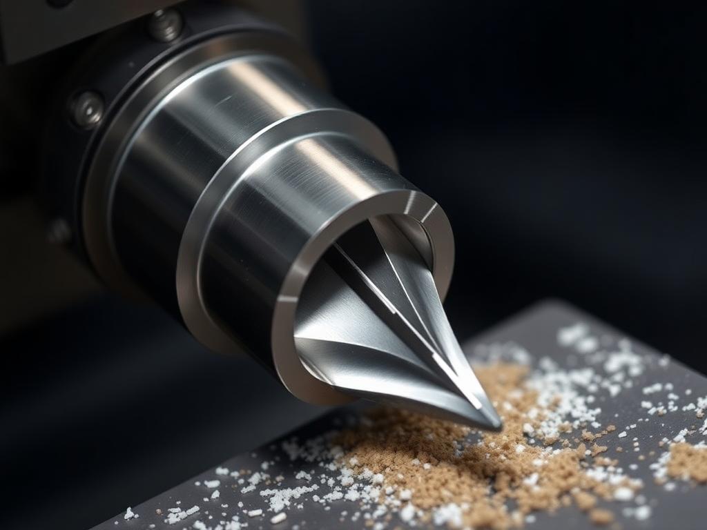
Can you mill a dowel pin with carbide cutter
The Ultimate Guide to PCB Depaneling Solutions: Advanced Manufacturing Technology for Electronics Industry
In today’s rapidly evolving electronics manufacturing landscape, efficient PCB depaneling is crucial for maintaining high-quality production standards. This comprehensive guide explores cutting-edge PCB depaneling solutions, from router machines to laser systems, helping electronics manufacturers optimize their production processes.
Why is Professional PCB Depaneling Critical for Modern Electronics Manufacturing?
The electronics industry demands precision and reliability in PCB separation processes. Modern PCB depaneling solutions offer:
- Superior accuracy with tolerances down to 0.0005″
- Reduced waste and higher yield rates
- Faster production cycles
- Protection of sensitive components
Learn more about our advanced PCB Router Machine solutions
What Are the Leading PCB Depaneling Technologies Available Today?
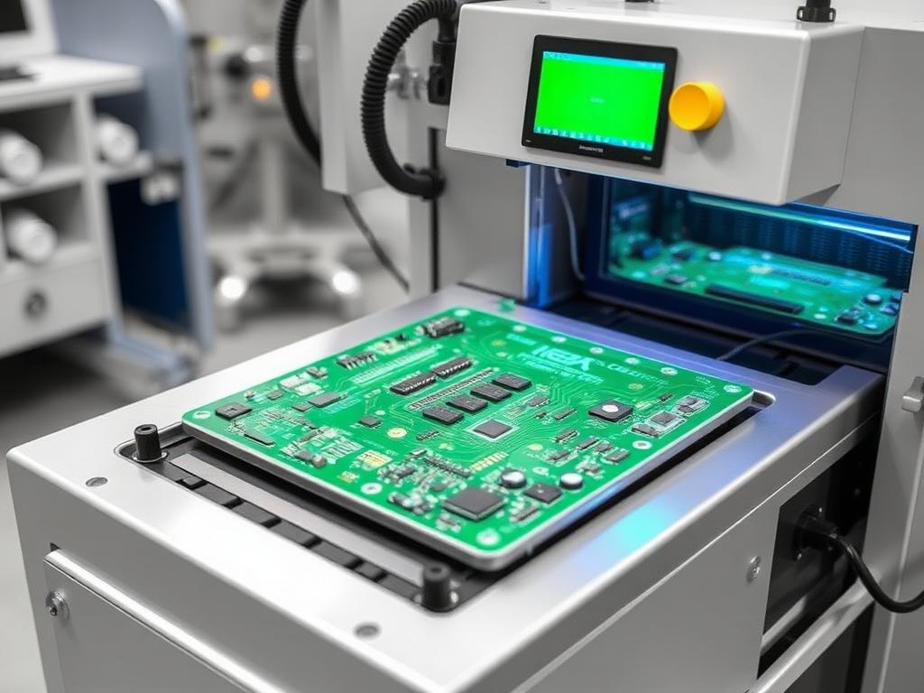
1. Router-Based Depaneling Systems
- High-precision routing capabilities
- Suitable for complex PCB shapes
- Minimal stress on components
- Explore our GAM330AD In-Line Automatic PCBA Router Machine
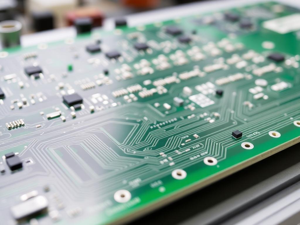
2. V-Groove Depaneling Technology
Modern V-groove systems offer:
- Clean, precise cuts
- High-speed processing
- Ideal for pre-scored PCBs
- Check out our advanced V-Groove solutions
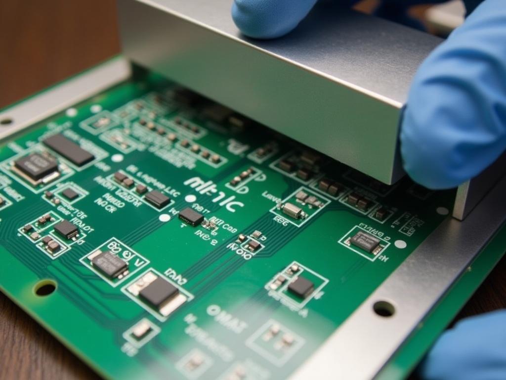
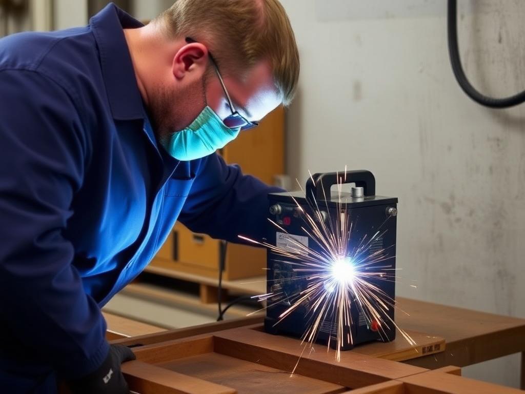
3. Laser Depaneling Systems
Benefits include:
- Contact-free processing
- Minimal mechanical stress
- Perfect for flexible PCBs
- Exceptional precision
How to Choose the Right PCB Depaneling Solution?
Consider these key factors:
- Production volume requirements
- PCB material and thickness
- Component proximity to cutting edges
- Budget constraints
- Speed requirements
Contact our experts for personalized guidance
Case Study: Fortune 500 Success Stories
Our solutions are trusted by industry leaders:
- TP-LINK: 30% increase in production efficiency
- Xiaomi: Reduced defect rates by 40%
- Foxconn: Improved throughput by 25%
Advanced Features of Modern PCB Depaneling Equipment
| Feature | Benefit |
|---|---|
| Automatic Tool Change | Reduced downtime |
| Vision Alignment | Enhanced accuracy |
| IoT Integration | Real-time monitoring |
| Dust Collection | Cleaner environment |
Frequently Asked Questions
What is the maximum PCB thickness your machines can handle?
Our machines can process PCBs up to 3.5mm thick, depending on the model and material.
How do you ensure component protection during depaneling?
We utilize advanced stress-free cutting technologies and precise control systems.
What is the typical ROI period for your equipment?
Most customers achieve ROI within 12-18 months through increased efficiency and reduced waste.
Can your machines handle flexible PCBs?
Yes, we offer specialized solutions for both rigid and flexible PCB processing.
Industry-Leading Support and Service
- 24/7 technical support
- Comprehensive training programs
- Preventive maintenance services
- Rapid response times
Discover our complete range of PCB depaneling solutions
Key Takeaways:
• Advanced PCB depaneling solutions increase production efficiency • Multiple technology options available for different requirements • Trusted by leading electronics manufacturers worldwide • Comprehensive support and service network • Proven ROI and performance benefits
Ready to optimize your PCB production process? Contact our experts for a customized solution that meets your specific requirements.