![]()

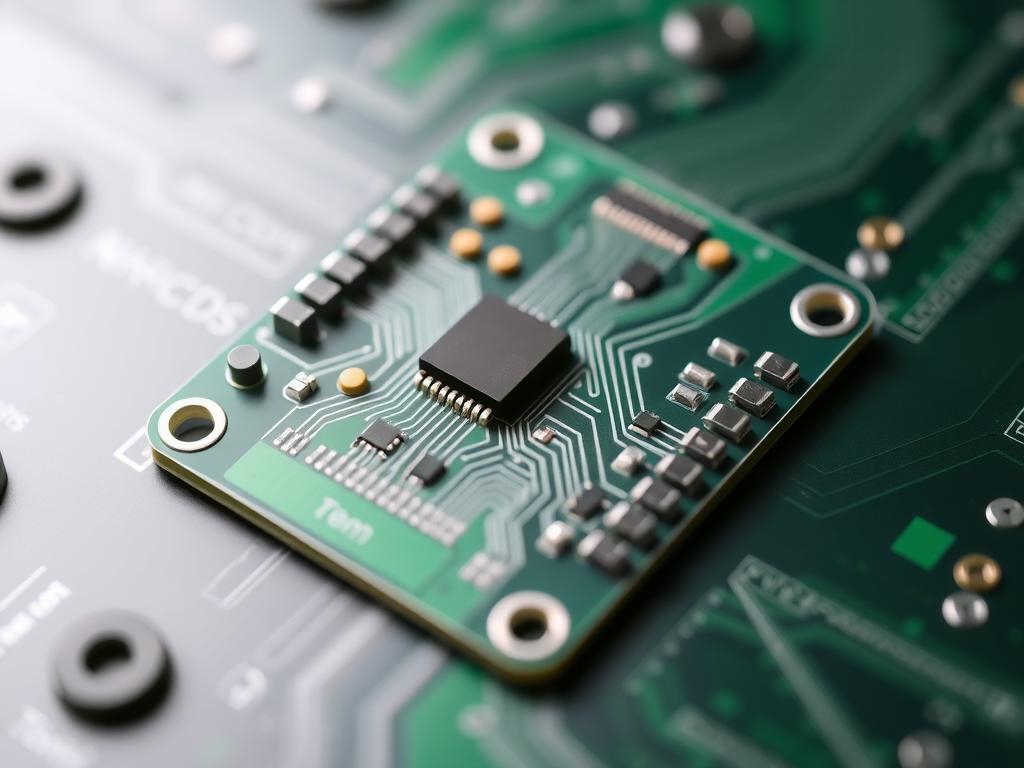
PCB depaneling for wearable technology
PCB Depaneling: Choosing the Right Method for Precision Circuit Separation
Hey there! If you’re in the world of electronics manufacturing, you know that creating a 印刷電路板(PCB) is only half the battle. The process of separating those 多氯聯苯 from a larger panel, known as PCB分板, is just as critical. This article dives deep into the various methods of PCB depaneling, particularly focusing on the precision and versatility offered by 雷射 technology, and will help you understand why it’s a game-changer for modern electronics. With my 20 years of experience in the field, you’ll get insights that only come from working with the best, including giants like TP-LINK, Canon, and Foxconn. This is your go-to guide to selecting the perfect depaneling solution for your unique needs.
Detailed Explanation
1. What is PCB Depaneling and Why is It Crucial?
PCB分板, also called singulation, is the 去除的過程 個人 印刷電路板 from the larger panel in which they are pcbs are typically manufactured. You see, pcbs are typically produced in a larger panel format that contains multiple boards. This makes the 印刷電路板組裝 process more efficient, but at the end, you have to separate boards 進入 individual circuits. This step is absolutely critical because improper depaneling can lead to cracks, 焊接 joint damage, or even delamination of the 基材, which can have a serious impact on product reliability. The 製造工藝 relies heavily on the precision and speed of the 分板工藝.
Think of it like this, you’ve spent time and resources designing and manufacturing a complex system. You wouldn’t want to risk damaging your perfectly produced 印刷電路板 at the last stage of the 製造工藝. That’s why choosing the correct 分板法 is not just about separating individual printed circuit, it’s about ensuring the quality and longevity of your electronic devices.
2. What are the Traditional Depaneling Methods?
Before the advent of advanced 雷射 technology, traditional methods like V-groove cutting, die-cutting, and punching were the standard. Each of these cutting methods has its advantages and disadvantages, often depending on the type of pcbs used and the desired volume. V-groove cutting involves creating grooves in the panel that are then snapped apart. Die-cutting uses a sharp tool to cut through the 印刷電路板 material and a 沖床 is used to separate the boards. While these methods can be suitable for some pcb applications, they often involve 機械應力 which can be problematic with more delicate components or intricate designs.
For instance, V-groove cutting, while being a relatively lower cost option, is limited to straight-line cuts and can produce a rough cut edge. Die-cutting, another option used for PCB切割, is better for complex shapes, but it’s typically suited to high volume runs and requires very specific tooling, making it less flexible. These traditional methods can also lead to stress on the board, potentially damaging the 焊點 and compromising the integrity of the 電子元件. This is why the industry is leaning more towards 雷射路由 和 雷射切割.
3. What are the Advantages of Laser Depaneling?
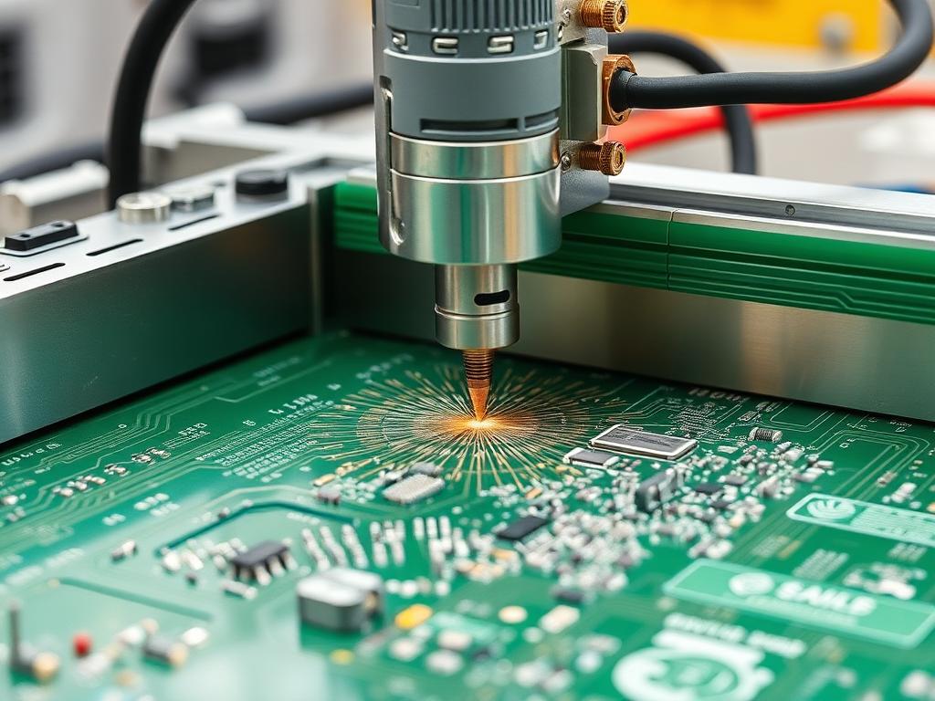
雷射分板 has revolutionized the 印刷電路板 industry. Why? Because a laser system offers unparalleled precision, speed, and flexibility. Unlike mechanical methods, a 雷射 uses a non-contact approach, directing a highly focused beam of light to vaporize material along a predefined 切割線. This means there is minimal 機械應力 於 印刷電路板, greatly reducing the risk of damage to the 電路 or other sensitive components.
Another huge advantage is the ability to cut intricate and complex shapes with a very narrow kerf width, which is impossible with traditional tools. 雷射切割 also offers very high 切割質量, leaving a clean and smooth edge. This level of accuracy is especially crucial for modern electronics that demand high precision and delicate handling. Furthermore, 雷射分板 can be used on a variety of materials, including flex pcbs 和 rigid flex, making it a very adaptable solution for various production needs. It is quickly becoming the preferred 分板方法 在 印刷電路板製造. We have seen a massive shift in the demand for 雷射 解決方案。
4. Why Choose Laser Over Other PCB Cutting Techniques?
When we talk about the evolution of pcb depaneling, it’s clear that 雷射 technology is at the forefront. Traditional methods such as mechanical routing and die-cutting can introduce 機械應力 on the board, which is a huge problem for high-density or delicate 多氯聯苯. 雷射分板 offers a non-contact solution, eliminating this issue.
Consider the manufacturing of smartphones and other modern 電子設備 with compact and highly integrated components. These devices rely on very small and tightly packed 電子元件. The precision of a 雷射 allows you to work with these components without worrying about damage or contamination, offering superior 切割質量. Additionally, the ability to cut complex shapes and curves with a 雷射 offers much more flexibility in design and 印刷電路板 layout compared to the constraints of traditional cutting systems。為了 applications that require intricate cuts, a 雷射 is a must-have. In short, it is the only 切割方法 that delivers the accuracy, precision, and flexibility needed in modern electronics manufacturing.
5. What Types of PCBs Benefit Most from Laser Routing?
Laser routing shines particularly bright when we talk about 柔性電路板 materials, rigid flex, and multilayer boards. These materials, often made from 聚醯亞胺 or similar flex materials, are sensitive to 機械應力 and can easily delaminate if handled roughly. 雷射分板 is the ideal method here, as it uses a focused 雷射光源 分開 individual circuits without making physical contact with the board, which makes it perfect for flex pcbs.
The precise control offered by a 雷射 also makes it an ideal solution for small pcbs that have very tight tolerances. It offers an advantage for high-density 多氯聯苯, where even the slightest 板上的應力 could cause damage. 雷射切割 can also handle complex contours and intricate designs with ease. If you’re working with complex or fragile 印刷電路, then 雷射分板 is probably the best solution for you. Additionally the high speeds that can be achieved, lead to higher 吞吐量 of products.
6. How Does Laser PCB Depaneling Reduce Mechanical Stress?
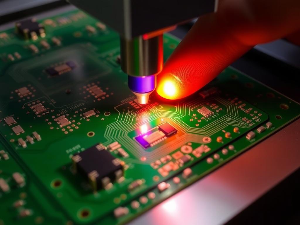
The key advantage of using a 雷射 為了 PCB分板 lies in its non-contact nature. Unlike mechanical methods that involve physical force, a 雷射 works by directing a highly focused beam of light that vaporizes the material along the 切割線. This means there is minimal 機械應力 應用於 印刷電路板. When you use traditional tools, you run a higher risk of micro-fractures, 焊接 joint damage, and delamination. All these can lead to decreased reliability and longevity of your product.
Another benefit to using a 雷射 is the very precise 切縫 that can be achieved. The 聚焦光斑尺寸 的 雷射 results in a very narrow 切縫, minimizing the area of material affected by the 切割工藝. This becomes critical when handling closely packed components. The non-contact nature of 雷射PCB分板 not only reduces 機械應力 but also minimizes the risk of dust and contamination, ensuring a much 清潔度 manufacturing process. With a 雷射 solution there is no wear and tear of the tools, such as cutting blades or similar.
7. What Are the Key Components of a Laser System for PCBs?
一個典型的 laser pcb depaneling system consists of several key components that work together to deliver the precise cutting process. At the heart of the system is the 雷射光源, which can be a CO2 雷射, a fiber 雷射,或一個 紫外線雷射. The type of 雷射 depends on the specific application and the type of 多氯聯苯 being processed. 紫外線雷射 is commonly used in the electronics industry because of its very small wavelength and 聚焦光斑尺寸 and the very low heat it generates.
Other essential components include the optical system, which guides and focuses the 雷射 beam; a motion control system, which precisely positions the 雷射 over the 印刷電路板; and a vision system, which helps align the 雷射 path with the design. Safety features, such as enclosures and interlocks, are also crucial for operating 雷射切割 equipment safely. The performance of a laser pcb depaneling system heavily relies on the quality and interaction of these key components. In summary, a system is more than just a 雷射, it’s a carefully engineered machine.
8. What About Lower Cost Alternatives for PCB Depaneling?
儘管 雷射分板 offers superior performance, traditional methods like V-groove cutting and 沖床 are still used because of their lower cost and relative simplicity. These methods are appropriate for simpler designs and large-volume runs where ultimate precision isn’t necessary. V-groove cutting, for example, relies on scoring lines on the 印刷電路 board and then breaking them apart. This method is ideal for straight lines and is often used for applications that require a basic, fast 分板工藝.
Similarly, die-cutting uses a specialized 工具 來削減 印刷電路板 from the larger panel. While these methods are lower cost, they do have limitations. They often generate 機械應力, are not suitable for intricate designs, and may result in a lower 切割質量. Therefore, while traditional methods might initially seem like a lower cost option, you must weigh the long-term impact on product quality and reliability as well as consider the total 製造工藝 costs. If your 電路 boards require precision and complex shapes, it is always worth considering 雷射PCB分板.
9. What is the Role of Laser in Wearable Technology Manufacturing?
The rise of wearable technologies, such as smartwatches and fitness trackers, has created a new demand for precision manufacturing techniques. These devices are characterized by their small size, complex internal components, and use of 柔性電路板. 雷射分板 has become an essential process in the production of these devices. The precise control and non-contact nature of 雷射 technology allows for cutting delicate flex pcbs without causing damage, which is essential for their reliable performance.
With the trend towards smaller and more functional wearables, 雷射路由 offers the flexibility and precision necessary to meet this need. For example, the small form factor of these devices requires the ability to cut very tight and complex shapes while avoiding any 板上的應力 or surrounding 電子元件. This is why the demand for high quality laser pcb depaneling systems is growing rapidly with the growth of the internet of things 和 wearable technologies.
10. How Can Our Depaneling Systems Meet the Demands of Today’s Manufacturing?
As a world-leading manufacturer of 分板系統, we at PCB Depaneling understand the challenges of modern electronics production. Our product range includes advanced laser pcb depaneling systems such as the DirectLaser series, which are designed to meet the stringent requirements of high-precision applications. We offer solutions for various production needs. Whether it is high volume 印刷電路板製造 or more intricate design. Our 雷射系統 are known for their reliability, precision, and efficiency, ensuring that our customers can achieve the best possible outcomes.
We also offer V-groove solutions and punching machinery, providing a range of options for every budget. We can help you choose the right 分板法 that matches your production goals. For example, we offer a comprehensive range of products including:
- GAM 380AT PCB 底部分板機 for automatic 印刷電路板 分離。
- ZM30-ASV 全自動鋸式V型槽PCB分板機 for high volume production.
- ZM10T & 15T PCB & FPC 沖切機 for simpler designs.
- 這 DirectLaser H5 PCB-FPC雷射切割機 for high precision cuts.
我們的 laser pcb depaneling systems are used by some of the biggest names in the industry, including TP-LINK, Canon, BYD, Flex, TCL, Xiaomi, Lenovo, OPPO, HONOR, and Foxconn. We take pride in supporting the leading innovators by providing solutions that exceed expectations. Our goal is to help you achieve the perfect balance of precision, speed, and cost efficiency.
常見問題解答
- What is the main difference between laser and mechanical PCB分板? The main difference is the nature of the 切割工藝. 雷射分板 is a non-contact method that minimizes 機械應力, while mechanical methods rely on physical force and can cause damage to sensitive 焊接 joints and other components.
- 能 雷射切割 handle flex pcbs?是的, 雷射切割 is especially well-suited for flex pcbs due to its non-contact nature and ability to make precise cuts on delicate flex materials without causing delamination or damage.
- 是 雷射分板 more expensive than traditional methods? While the initial investment for a laser system can be higher, the long-term benefits of 雷射分板—including higher precision, minimal damage, and increased flexibility—often make it a more cost-effective option for high-quality, complex 多氯聯苯 和 電子元件.
- 需要什麼樣的維護 雷射系統? The maintenance of 雷射系統 mainly involves keeping the optics clean and periodically checking the alignment of the 雷射 beam. The frequency of maintenance depends on the usage and the working environment of the machine. We also offer maintenance contracts if you want peace of mind.
- What are the typical applications that require 雷射PCB分板? 雷射分板 is commonly used in the manufacturing of smartphones, wearables, high-density boards, and any other applications that require high precision and delicate material handling.
結論
Choosing the right method for PCB分板 is crucial for the quality and reliability of your electronic products. While traditional methods may offer lower cost solutions, 雷射分板 stands out for its superior precision, flexibility, and minimal 機械應力, making it the preferred choice for modern electronics manufacturing. With 20 years in the field, I have seen firsthand how 雷射 technology has transformed the 印刷電路板 industry. Our 分板系統, used by leading tech companies, demonstrate our commitment to quality and innovation. We have solutions for all, whether you are a large plant or a smaller operation.
Here’s a quick summary of what we’ve discussed:
- 雷射分板 offers non-contact precision cutting, minimizing 機械應力.
- Laser routing is ideal for complex shapes, flex pcbs, and high-density boards.
- Traditional methods are lower cost but lack the precision of 雷射切割.
- Our products have been proven by leading electronic companies and are in use all over the world.
- We provide comprehensive 分板解決方案 tailored to your specific needs.
To learn more about how our 分板系統 can benefit your production process, I invite you to explore our range of products. Contact us today and let our expertise and support help you achieve manufacturing excellence. Don’t settle for less when it comes to precision, choose a proven partner for PCB分板. We are here to support your goals. If you would like to learn more about our products, please check out our GAM 360AT 線上 PCB 分板機, or our GAM 330AT 線上自動 PCB 銑床. For those of you working with flex, be sure to see our ZM10T & 15T PCB & FPC 沖切機. Also check out our ZM30-ASV 全自動鋸式V型槽PCB分板機, or our DirectLaser H5 PCB-FPC雷射切割機.