![]()

V-Groove Depaneling for Consumer Electronics: Fast Separation Without Slowing the Line
If your SMT line is getting backed up at the very end—and you’re seeing random MLCC failures popping up in the field—we need to talk about the elephant in the room: stop snapping panels by hand. It’s the fastest way to kill your yield. If you want to actually hit your numbers without shipping defects, you’ve got to automate. For your standard FR4 boards, a solid v-cut pcb depaneling system is the move. It’s fast, clean, and gets the job done. But if you’re dealing with high-density stuff, flex circuits, or anything super sensitive to stress? Don’t even risk it—go with a pcb laser cutting machine. It’s the only way to get zero-stress cuts every single time.
By matching the specific design of your panelized board with the correct automated machinery, we can help you cut your separation cycle time down to mere seconds. More importantly, you will eliminate the mechanical stress that causes hidden cracks in your ceramic capacitors, drastically improving your long-term product reliability. In our years of experience engineering factory floor solutions, we have learned that the “cheapest” manual method is actually the most expensive when you factor in field failure rates. Here is exactly how we recommend you optimize your production line to maximize your ROI.
The Hidden and Expensive Cost of Manual Separation
When an operator manually bends a V-scored panel to snap it, they are introducing sheer mechanical torque directly into the fiberglass substrate. This flexing action causes micro-cracks in brittle surface-mount components, particularly Multilayer Ceramic Capacitors (MLCCs). The most terrifying part about these micro-cracks is that they are practically invisible. They will often pass your end-of-line electrical testing without a problem, only to fail weeks or months later in the hands of the consumer due to moisture ingress or thermal cycling.
As solutions experts, we have seen companies lose entire profit margins to warranty claims and product recalls because of this exact issue.
According to a study measuring solder joint stress across different methods, manual breaking generates stress peaks exceeding 1000 µƐ (microstrain). In stark contrast, utilizing proper automated equipment like a CNC pcb router machine keeps that stress below 250 µƐ. That massive reduction in strain is the difference between a reliable product and an expensive warranty claim.
V-Cut PCB Depaneling: The High-Volume Champion
For straight-line, rectangular boards—think LED lighting strips, power supplies, or simple consumer IoT devices—V-scoring is the ultimate tool for balancing cost and speed. It is an industry workhorse that we consistently recommend for high-volume, low-complexity manufacturing.
How to Properly Specify Your V-Score Parameters
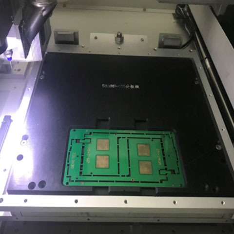
The V-scoring process happens early during bare board fabrication. The manufacturer uses angled blades (usually 30°, 45°, or 60°) to cut V-shaped grooves into both the top and bottom of the panel. For a standard 1.6mm thick FR4 board, the golden engineering rule is to cut 1/3 of the depth on top, 1/3 on the bottom, leaving exactly 1/3 of the web material (about 0.3mm to 0.5mm) in the middle[2].
This residual web is crucial. It holds the panel together seamlessly through the pick-and-place machines and the reflow oven but is weak enough to be separated easily at the end of the line.
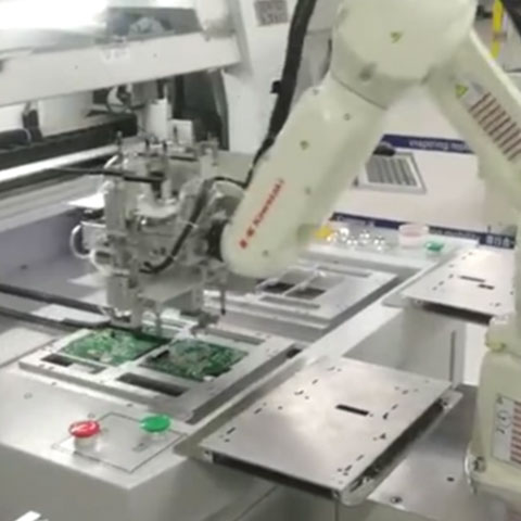
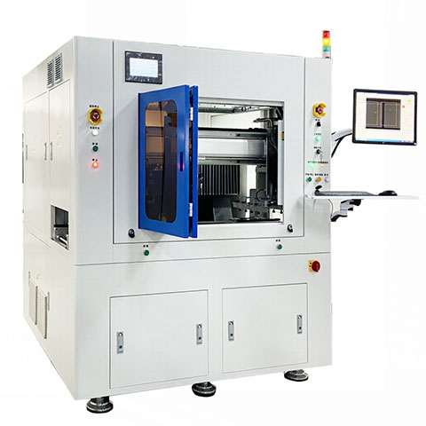
To process these boards rapidly and safely on the factory floor, you must use a motorized v-groove depaneling separator. This equipment uses precision rotary blades made of high-speed steel to glide horizontally through the groove. Because the machine specifically targets the connecting web, it splits the board using localized cutting force. There is zero bending, zero twisting, and zero torque applied to your components.
Expert Best Practice: Enforce Strict Component Clearance ZonesWe always tell our clients that perfect separation starts in the CAD software. Enforce strict Design for Manufacturing (DFM) keep-out rules early. Keep standard SMD chip components at least 1.5mm away from the V-groove centerline. For sensitive ceramic components (MLCCs), push them back to at least 2.0mm to 3.0mm, and for BGA packages, maintain a strict 3.0mm keep-out zone to prevent solder joint fatigue caused by dynamic stress.
The Ultimate Zero-Stress Upgrade: Laser Depaneling
V-scoring is fantastic, but it has a definitive limitation: it is strictly restricted to straight lines spanning edge-to-edge. If you are manufacturing High-Density Interconnect (HDI) boards, thin Flexible Printed Circuits (FPC), complex rigid-flex boards, or medical-grade devices, mechanical separation is no longer a viable option.
When absolute precision and zero damage are required, a laser depaneling machine shifts from being a “nice-to-have” luxury to a mandatory factory upgrade.
Why Lasers Dominate High-End Manufacturing
A laser system (utilizing either UV or CO2 technology) employs a “cold ablation” process. It vaporizes the FR4 or Polyimide material without making any physical contact with the board. No physical contact means zero friction, zero vibration, and absolutely zero mechanical stress.
Furthermore, while the initial Capital Expenditure (CapEx) of a laser system is higher, we always point factory owners to the massive, hidden ROI: Substrate Material Savings.
A traditional mechanical router bit requires a cutting channel (kerf width) of anywhere from 1.0mm to 3.0mm. In contrast, a modern UV laser boasts an incredibly narrow kerf width of just 25 µm to 40 µm. This microscopic cutting channel allows your layout engineers to pack individual circuits practically edge-to-edge on the panel array. When you are processing expensive ceramic substrates or multi-layer boards, this can yield up to a 30% saving on bare board costs, paying off the machine faster than you might expect.
Finding the Middle Ground: Routers and Punching Dies
Not every EMS factory needs a laser, and not every PCB layout allows for V-scoring. For mixed production environments, we rely on CNC and mechanical alternatives to get the job done safely.
The Versatility of a PCB Router
If your boards have complex, irregular shapes, internal cutouts, or utilize “mouse bite” tab routing, CNC routing is highly flexible. By simply uploading a new cutting path via software, the spindle can mill out almost any contour. Modern machines offer excellent edge quality with a repeatability of ±0.02mm. Just remember that routers grind material away, so you must ensure the equipment has a high-grade vacuum extraction system to manage the residual fiberglass dust.
The Speed of a Punching Machine
For massive volumes of simple, non-rectangular shapes, a punching machine is unmatched in raw speed. It uses custom-made metal dies to stamp out the boards in a single stroke. It generates minimal dust and is incredibly fast. However, it requires a high upfront tooling cost for the die. Because you must machine a new die every time your PCB layout changes, we only recommend this method for products with a very long lifecycle.
Expert Best Practice: Move from Offline to Inline AutomationDo not let your high-speed SMT line wait on human operators. We highly recommend integrating your depaneling equipment directly inline at the end of the conveyor belt. By utilizing CCD machine vision to auto-align cuts and robotic pick-and-place arms to stack the finished boards into trays, you establish a continuous, uninterrupted Takt time. This eliminates human handling errors, reduces operator headcount, and creates a true Smart Factory workflow.
Executive Summary: Depaneling Methods Compared
To help you make a fast, data-driven decision for your factory floor, review our technical comparison matrix below:
| Depaneling Method | Best Factory Application | Component Stress Level | Required Clearances / Kerf Width |
| V-Cut Separator | High-volume, straight rectangular cuts | Low (Highly Localized) | N/A (Requires 1.5 – 3.0mm keep-out zone) |
| PCB Router | Complex shapes, high-mix production | Very Low (<250 µƐ) | 1.0mm – 3.0mm routing channel |
| Laser Cutting | FPC, HDI, sensitive MLCC components | Zero (No Physical Contact) | Ultra-thin (<40 µm)[4] |
| Punching Die | Fixed designs, massive mass volume | Medium | Dictated by custom die geometry |
Frequently Asked Questions (FAQ)
Q1: Can we use V-scoring for flexible circuits (FPC) and ultra-thin boards?
We strongly advise against it. Flexible printed circuits and ultra-thin rigid boards (under 1.0mm thick) lack the structural rigidity required for mechanical V-scoring. The localized force of the blade will cause the material to warp and buckle. For FPCs, you must use a laser system or a dedicated die-punching machine to ensure a clean, stress-free cut.
Q2: Does an automated V-cut machine produce harmful fiberglass dust?
It produces very minimal dust. Because the rotary circular blade splits the remaining fiberglass web rather than aggressively grinding it away (which is what a CNC router bit does), it generates drastically less airborne debris. This keeps your PCBA environment clean and protects exposed solder pads.
Q3: How much space do we realistically need to leave between components and the cutting edge?
For V-scoring, we recommend an absolute minimum of 1.5mm for standard SMDs and 2.0mm to 3.0mm for sensitive MLCCs and BGAs to prevent micro-cracks. For laser cutting, because there is no mechanical stress transferred to the board, you can place components much closer to the edge, sometimes within 0.1mm of the cut line.
Q4: CO2 or UV laser—which one’s better for cutting boards?
Depends on what you’re trying to do. Look, a CO2 laser is your workhorse. It’s fast and it’s cheap, but it’s “dirty.” You’re gonna get a wider cut and some charring on the edges. If your boards can handle a little toastiness, go for it.
But if you’re messing with high-density stuff or rigid-flex? You need a UV laser. It’s a “cold cut”—no heat, no charring, just a razor-thin line. It’s the only way to handle sensitive components without stressing ’em out. It costs more, but you won’t be throwing boards in the scrap bin.
Q5: What happens if our PCB fabricator makes the V-score web thickness too thin?
If the fabricator cuts too deep and leaves a web thinner than 0.3mm (on a standard 1.6mm board), the panel becomes overly fragile. It may prematurely snap during handling or sag violently while traveling through the extreme heat of the reflow oven. This sagging will ruin your solder joints before the board even reaches the separation stage.