![]()

Передові методи депанелювання друкованих плат
Від ручного до лазерного: революційне депанелювання друкованих плат для максимальної ефективності
Протягом двох десятиліть я був занурений у світ друкованих плат (друкована платаs), на власні очі спостерігаючи за їхньою еволюцією процес депанеліВід перших днів кропіткого ручного розділення до найвищої точності лазер технології, це була надзвичайна подорож. Якщо ви берете участь у друкована плата виробництво, особливо великосерійне виробництво, ефективність і точність вашого депанелювання друкованих плат методи критичні. Ця стаття заглиблюється в трансформаційний перехід від традиційних, часто стресових, методів до обтічної сили лазерне депанелювання, і чому використання цих досягнень має вирішальне значення для сучасного конкурентного середовища. Розуміння цих способи депанелювання друкованих плат має важливе значення для оптимізації вашої виробничої лінії, і тому цю статтю обов’язково потрібно прочитати всім, хто працює в електроніці.
Опис статті: Навігація у світі депанелювання друкованих плат
Ось дорожня карта того, що ми досліджуватимемо, щоб допомогти вам зрозуміти найкраще метод депанелі для ваших потреб:
- Які загальні методи депанелювання друкованих плат та їхні обмеження?
- Чому Лазерне депанелювання Набирає популярності як бажаний PCB Техніка поділу?
- Як робить Лазерна Технологія забезпечує точність Депанелювання друкованих плат Процес?
- Коли це a PCB маршрутизатор Машина ідеальний вибір для PCB Розлука?
- Наскільки значно Лазерне депанелювання Покращення виробництва Пропускна здатність?
- Яка роль робить ефективним PCB Panelization Грати в оптимізоване депанелювання?
- Є удар Методи, які все ще актуальні в сучасному світі Депанелювання друкованих плат?
- Як правильно PCB Panelization Вплинути на успіх депанелі?
- Які ключові міркування забезпечують Гарантія якості у вашому процесі депанелі?
- Як вибрати правильний метод Депанель і досягнути Ефективне депанелювання?
- Які фактори слід враховувати, коли Вибір правильного методу депанелі?
Розшифровка методів депанелювання та їх недоліки
За ці роки я бачив різне метод депанеліприходять і йдуть. На початку це було часто ручне депанель, повільний і трудомісткий процес, схильний до помилок і механічне навантаження на делікатному схема. Уявіть, що ви намагаєтеся окремо індивідуальні pcb від а більша панель вручну – ризик пошкодження компонентів або матеріал друкованої плати сам по собі був значним. Потім з’явилися такі методики v-оцінка, де a v-подібний паз попередньо забивається на друкована плата, що дозволяє контролювати перерва уздовж лінії. Хоча це швидше, ніж ручні методи, v-оцінка ще вводить механічне навантаження і може залишити шорсткі краї. Використовуючи a удар натисніть, щоб змусити індивідуальна друкована схема дошки з панель друкованої плати був інший підхід, придатний для простіших конструкцій, але часто призводить до деформації та обмежень дизайн друкованої плати. Навіть використовуючи гострі леза на одній частині а підтримка з іншого боку може викликати небажаний стрес і невідповідності. Ці традиційні способи депанелювання друкованих плат, а іноді економічно ефективний для малосерійного виробництва часто намагаються задовольнити вимоги високого пропускна здатність і жорсткі вимоги до якості в сучасному виготовлення друкованих плат.
Розвиток лазерного депанелювання: точність і ефективність на новому рівні
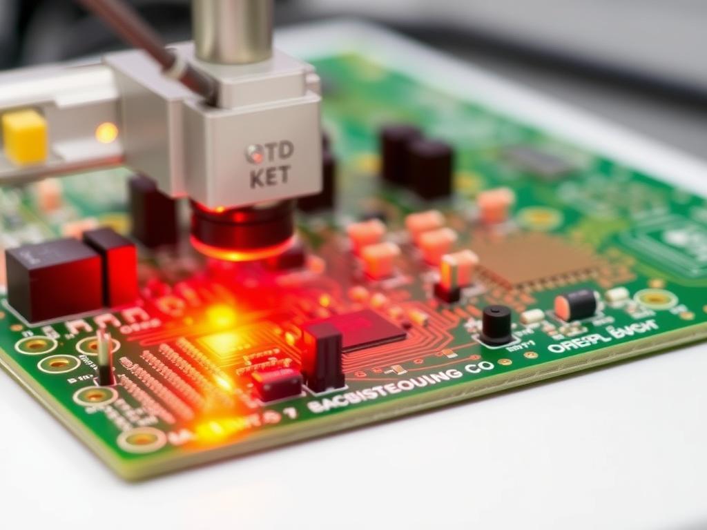
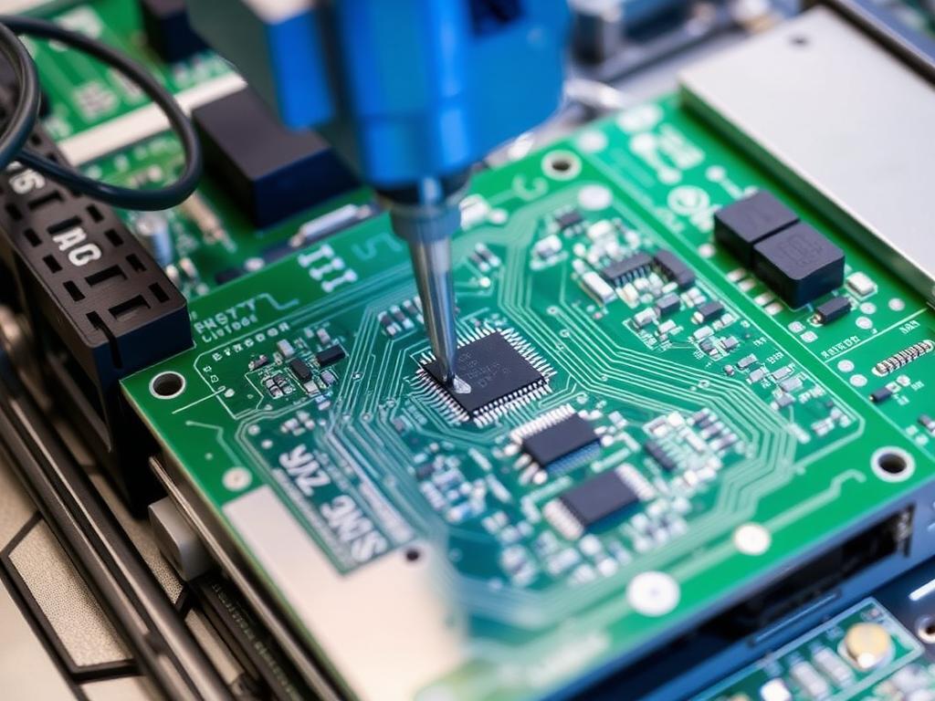
Поява лазерне депанелювання здійснив справжню революцію в галузі. Замість фізичної сили, високо сфокусований лазерний промінь точно прорізає друкована плата, залишаючи чисті, гладкі краї та усуваючи майже всі механічне навантаження. З моєї точки зору, спостерігати цей перехід було неймовірно. Здатність лазер технологія точного дотримання складних контурів і окремо складний дизайн дошки не має собі рівних. The лазерне різання процес є безконтактним, тобто до нього не прикладається пряма сила друкована плата, що значно знижує ризик пошкодження. Це особливо важливо для чутливих і тонких компонентів товщина друкованої плати. Незалежно від того, жорстка чи гнучка підкладка схеми, лазерне депанелювання пропонує рівень точність і якість що традиційні методи просто не можуть зрівнятися. Штраф ширина пропилу досяжна з лазерні системи також дозволяє щільніше панелізація, максимізуючи використання матеріалу з a більша панель. Цей стрибок у технології усуває багато обмежень старих технологій виготовлення лазер головний претендент на ефективність і високу якість депанель.
Лазерна точність: ближчий погляд на передовий край
Магія лазерне депанелювання полягає в його високій точності. Дрібно сфокусований лазерний промінь, часто a УФ-лазер за його здатність прорізати різні матеріал друкованої платиs чисто, видаляє матеріал по бажаному шляху. Подумайте про це як про мікроскопічний скальпель, керований точним програмним керуванням. Це процес різання є неймовірно точним, гарантуючи, що індивідуальні друк друковані плати є окремоd точно так, як розроблено. The потужність лазера, швидкість і розмір сфокусованої плями можна налаштувати на основі товщина друкованої плати і матеріал, що дозволяє оптимізувати для різних тип друкованої плати. Цей рівень контролю зводить до мінімуму сміття та зони впливу тепла, що має вирішальне значення для підтримки цілісності схема. Попрацювавши з різними лазерні системи, я можу засвідчити їх стабільну продуктивність і здатність впоратися навіть із найскладнішими друкована плата вздовж хитромудрі обриси. Використання коротші ультрафіолетові хвилі додатково підвищує точність і зменшує термічні ефекти, що робить його ідеальним для делікатних технологія друкованої плати.
Коли маршрутизатор друкованої плати все ще сяє?
Незважаючи на прогрес у лазерне депанелювання, pcb маршрутизатор машини залишаються цінним інструментом у певних ситуаціях. А маршрутизатор використовує спінінг фрезерний біт фізично прорізати друкована плата. Хоча він представляє деякі механічне навантаження, сучасний pcb маршрутизатор машинаs пропонують високу швидкість і можуть бути економічно ефективний для особливих застосувань, особливо для більш товстих дощок або при роботі зі складними вкладка видалення. З мого досвіду, маршрутизатор машини перевершують ситуації, коли дизайн друкованої плати має легкодоступні шляхи маршрутизації. Вони також є добре налагодженою технологією з нижчим початкові капітальні вкладення порівняно з лазерні системи. Однак важливо враховувати ступінь зносу фрезерний біт, потенціал утворення пилу та обмеження щодо різання складних внутрішніх контурів порівняно з лазер методи. Ми пропонуємо асортимент PCB Router Machineрозроблено для ефективної та надійної роботи.
Підвищення продуктивності виробництва за допомогою лазерної технології
Одна з найбільш істотних переваг лазерне депанелювання є його вплив на виробництво пропускна здатність. Швидкість і можливості автоматизації лазерні системи значно скоротити час циклу порівняно з ручним або навіть ручним маршрутизатор-базовані методи. А лазер може швидко і точно розрізати друкована плата матеріалу, а вбудовані функції автоматизації дозволяють безперервно обробляти панель друкованої платис. Уявіть різницю між роз’єднанням дощок вручну та a лазер система без проблем відокремлюючи індивід дошки з високою швидкістю і точністю. Це збільшилося пропускна здатність безпосередньо перетворюється на збільшення обсягів виробництва та зниження виробничих витрат. Для великих заводів з обробки електронних виробів і навіть індивідуальних друкована плата гравці, які мають справу зі значними обсягами, забезпечує лазерна технологія чіткий шлях до підвищення ефективності. наш Лазерне депанелювання друкованих плат Рішення розроблені спеціально для максимізації вашого виробництва.
Вирішальна роль панелей друкованих плат в успіху депанелей
Ефективний друковані панелі is paramount for optimizing the процес депанелі, незалежно від спосіб різання використовується. Panelization refers to the arrangement of multiple індивідуальні pcb on a single manufacturing panel. Smart panelization techniques minimize material waste, improve handling efficiency during the виробничий процес, and streamline the процес відокремлення. для лазерне депанелювання, well-designed панелізація ensures optimal spacing for the сфокусований лазерний промінь and allows for continuous cutting without unnecessary interruptions. Similarly, for маршрутизатор methods, proper панелізація ensures accessibility for the фрезерний біт. Poor панелізація can lead to increased stress on the друкована плата, difficulties in separating individual printed circuit boards, and ultimately, reduced quality assurance. Therefore, careful consideration of панелізація є a crucial step in pcb manufacturing to ensure a smooth and efficient процес депанелі.
Punching Methods: A Look at Their Place in the Modern Era
Поки лазер і маршрутизатор technologies dominate high-precision депанель, удар methods still find application in certain niche areas. Using a dedicated машина для штампування pcb/fpc, individual boards can be вибитий з панелі using custom-designed tooling. This method is generally suitable for simpler board shapes and high-volume production of the same design. However, the force involved in ударing can introduce significant механічне навантаження, potentially damaging sensitive components. The tooling also needs to be precisely manufactured and maintained, and changes in board design require new tooling, adding to the економічно ефективнийness calculation. While not ideal for complex or delicate друкована платаs, удар methods can still be a viable option for specific, high-repetition applications where precision is less critical. We offer Машина для штампування PCB/FPCs for these specific needs.
How Panelization Shapes the Depaneling Outcome
The way you arrange your панель друкованої плати has a profound impact on the ease and success of depanelization. Think of it like this: a well-organized puzzle is much easier to take apart than a jumbled mess. Effective друковані панелі considers the метод депанелі that will be used. For instance, if using a лазер, the layout should provide clear, continuous paths for the лазерний промінь to follow. For маршрутизатор methods, sufficient space needs to be provided for the машина‘s cutting head to maneuver. The placement of вкладкаs or breakaway points also needs careful consideration. Poor панелізація can lead to increased механічне навантаження протягом поділ, making it harder to achieve clean breaks and potentially damaging components or the матеріал друкованої плати. Investing time in optimizing your panelization techniques є ключем найкращі практики to ensure a smooth and high-quality процес депанелі.
Ensuring Quality: The Cornerstone of Effective Depaneling
Quality assurance is paramount in the процес депанелі. Regardless of the метод депанелі used, the goal is to окремо в індивідуальні друковані плати without introducing defects or damage. With лазерне депанелювання, the precision of the сфокусований лазерний промінь minimizes stress and creates clean edges, inherently contributing to higher quality. Regular maintenance of equipment, whether it’s a laser system або a маршрутизатор, is crucial. Proper training for operators is also essential to ensure they understand the nuances of the chosen метод на практиці. Careful inspection of депанельований boards is a final step to catch any potential issues. For instance, checking for micro-cracks or residual burrs can help identify areas for process improvement. By focusing on точність і якість throughout the процес відокремлення, you can minimize scrap and ensure the reliability of your final product.
Choosing the Right Path: Selecting Your Ideal Depaneling Method
Вибір правильного методу депанелі is a critical decision that impacts your production efficiency, cost, and product quality. Consider the volume of your production, the complexity of your дизайн друкованої плати, the materials used, and your budget. For high-volume production requiring intricate cuts and minimal stress, лазерне депанелювання is often the superior choice. If you’re dealing with thicker boards or simpler designs and looking for a more established and potentially lower початкові капітальні вкладення, а pcb маршрутизатор машина might be suitable. For very high-volume, simple designs, удар methods could be considered. Ultimately, the best approach involves carefully evaluating your specific needs and weighing the pros and cons of each метод депанелі. We offer a comprehensive range of depaneling solutions, including laser, маршрутизатор, і удар machines, and our experienced team can help you navigate these choices.
Factors to Ponder When Choosing Your Depaneling Solution
Коли справа доходить до choosing the right depaneling solution, several factors come into play. Your production volume is a major consideration. High-volume environments often benefit most from the speed and automation of лазерні системи. The complexity of your дизайн друкованої плати is another key factor. Intricate shapes and internal cutouts are handled with greater ease and precision by лазер technology. The товщина друкованої плати і матеріал друкованої плати also influence the choice. Thicker boards might be more effectively processed by a robust маршрутизатор, поки лазер is excellent for a wide range of materials, including sensitive flex circuits. Your budget, including both the початкові капітальні вкладення and ongoing operational costs (like tooling for удар methods or фрезерний біт replacement), needs careful evaluation. Finally, consider the level of механічне навантаження that your components can tolerate. Лазерне депанелювання, with its non-contact approach, minimizes stress, making it ideal for sensitive electronics. By carefully weighing these factors, you can make an informed decision and select the метод депанелі that best aligns with your specific requirements.
Conclusion: Embracing Efficiency and Precision in PCB Depaneling
The journey from manual ламання рук з друкована платаs to the sophisticated precision of лазерне депанелювання reflects significant progress in виготовлення друкованих плат. As a leading депанелювання друкованих плат machine manufacturer, we’ve witnessed firsthand the transformative impact of these advancements on our customers, including industry giants like TP-LINK, Canon, BYD, Flex, TCL, Xiaomi, Lenovo, OPPO, HONOR, and Foxconn. Whether you opt for the speed and versatility of a лазер system, the established reliability of a маршрутизатор, or a specialized удар solution, the key is to choose a method that optimizes your production пропускна здатність, maintains high quality assurance, and minimizes механічне навантаження on your valuable схема. Embracing efficient and precise процес депанеліes is no longer a luxury but a necessity for staying competitive in today’s fast-paced electronics industry.
Ключові висновки:
- Лазерне депанелювання offers unmatched precision and minimizes mechanical stress.
- Машини для маршрутизації друкованих плат remain a viable option for certain applications, especially thicker boards.
- Ефективний друковані панелі is crucial for optimizing any метод депанелі.
- Careful consideration of production volume, board complexity, and budget is essential when selecting a depaneling solution.
- Prioritizing quality assurance throughout the depaneling process is paramount.
FAQs: Your Questions About PCB Depaneling Answered
What are the main advantages of using a laser for PCB depaneling? Laser depaneling offers high precision, minimal mechanical stress, clean cut edges, and the ability to process intricate board shapes efficiently.
Is laser depaneling suitable for all types of PCB materials? Yes, laser depaneling, particularly with UV lasers, can effectively process a wide range of PCB materials, including FR-4, flex circuits, and more.
How does a PCB router machine compare to laser depaneling in terms of cost? PCB router machines typically have a lower initial investment cost compared to laser systems, but factors like tooling and bit replacement should be considered in the long run.
What role does automation play in modern PCB depaneling? Automation significantly increases throughput and reduces manual handling, making the depaneling process more efficient and consistent, especially with laser and advanced router systems.
What factors should I consider when deciding between laser and router depaneling? Consider your production volume, board complexity, material types, budget, and the level of mechanical stress your components can withstand.
Ready to elevate your PCB depaneling process? Contact us today to explore the best solutions for your needs!
Explore our range of PCB Router Machines Learn more about our advanced PCB Laser Depaneling solutions Discover our efficient V-Groove Depaneling options See our durable PCB/FPC Punching Machines Explore our range of Automatic Equipment for streamlined production View our selection of high-quality Accessories