![]()

Гибкая разборка печатных плат
PCB Depaneling: A Comprehensive Guide to Separating Your Circuits
As someone who’s spent the last two decades immersed in the world of printed circuit boards, I’ve seen firsthand how critical depaneling is to the entire PCB manufacturing process. From rigid boards to the most delicate flexible pcbs, getting the separation process right is essential for quality and efficiency. This article will guide you through the various aspects of PCB depaneling, offering insights into methods, technologies, and why choosing the right approach can make or break your production. Whether you’re a seasoned professional or just starting, this comprehensive overview is for you. It’s a must-read because it breaks down complex processes into easy-to-understand explanations, highlighting practical aspects for your manufacturing needs.
What is PCB Depaneling and Why is it Crucial?
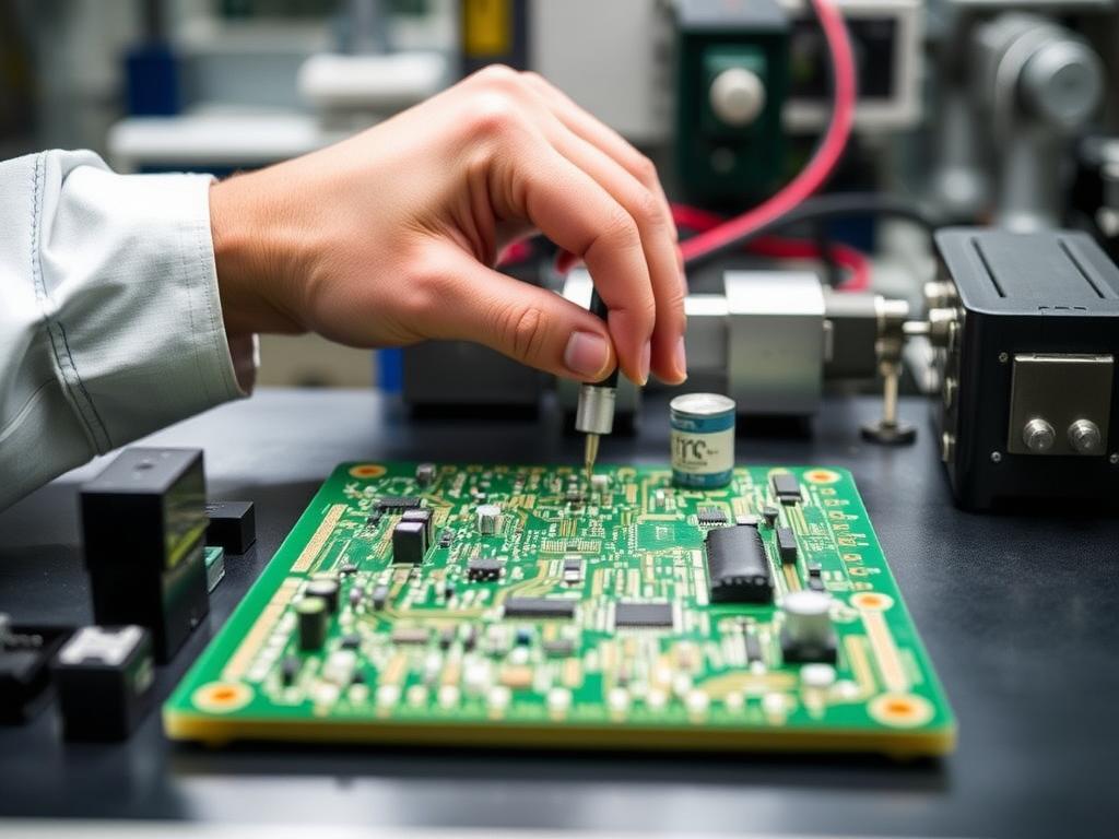
PCB depaneling is the separation process where individual circuit boards are cut out from a larger panel or array after the сборка печатной платы and soldering operations are completed. This is a critical step in the pcb manufacturing process because a single panel often holds multiple печатные платы to streamline production and reduce costs. Think of it like a sheet of cookies – you bake them all together but need to separate them at the end. The way you depanel or separate those boards is just as crucial as how they are manufactured. Without a proper depaneling technique, you risk damaging the final product, leading to scrap and increased costs, and that’s not something anyone wants. This process is also called singulation.
Having worked with various manufacturing plants for years, I’ve seen the impact of efficient depaneling firsthand. If you have uneven edges, damage to components, or excessive механическое напряжение on the board, all these issues can lead to defects. Therefore, choosing the correct depaneling method and using the right equipment is essential to maintain quality and consistency of your circuits. It’s a necessary step to get those individual boards ready for use in the final electronic devices.
What Are the Main Depaneling Methods Available?
Over the years, I’ve worked with several depaneling methods, and each has its unique use cases and suitability for different types of boards and production volumes. Here are some of the most common:
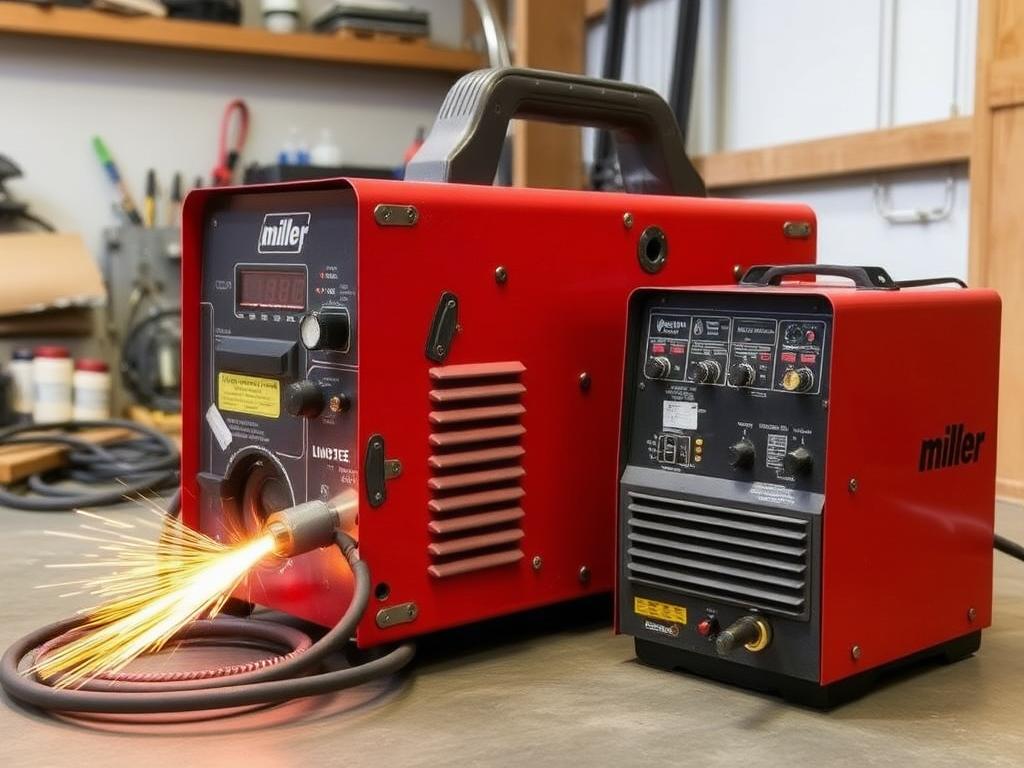
- Разделение V-образных канавок: This method involves using a blade to create a shallow groove on both sides of the board along the separation line. It’s commonly used for rigid pcb boards and is an inexpensive and simple solution. However, it is not suitable for designs with components very close to the board edge or for flex pcbs.
- Router Cutting: A router uses a high-speed rotating bit to cut along the separation line. It’s a popular method for both rigid and flexible pcbs due to its precision and ability to handle more complex shapes. I’ve seen it used for everything from simple rectangular boards to more intricate designs. It is more versatile but can create dust and requires fixture.
- Штамповка: This method employs a die and punch to quickly separate boards. It is more appropriate for simple designs and high production volumes. However, it’s less precise than other methods and is generally not recommended for circuits with delicate components. I’ve mostly seen it in high-volume, low-complexity production scenarios.
- Laser Cutting: A high-precision method that uses a laser beam to cut through the подложка печатной платы. This method is favored for flexible printed circuits and complex board outlines because it provides high accuracy with minimal механическое напряжение. Лазерное депанелирование is a more advanced technology that allows for intricate designs and delicate materials.
Each method has its own advantages and limitations, which is why it is critical to choose wisely. The table below summarizes the most common methods, which may help you make an informed decision, especially when considering which tool is used to create the individual boards.
Table 1: Comparison of Depaneling Methods
| Метод | Пригодность материала | Точность | Скорость | Расходы | Лучшее для |
|---|---|---|---|---|---|
| V-образная канавка | Rigid PCB, FR4 | Середина | Высокий | Низкий | Simple, straight separation lines |
| Фрезерная резка | Rigid & Flexible PCB | Высокий | Середина | Середина | Complex shapes, boards with components close to edge |
| Штамповка | Жесткая печатная плата | Середина | Высокий | Середина | High-volume production, simple designs |
| Лазерная резка | Flexible & Rigid PCBs | Высокий | Середина | Высокий | High-precision, intricate shapes, delicate boards |
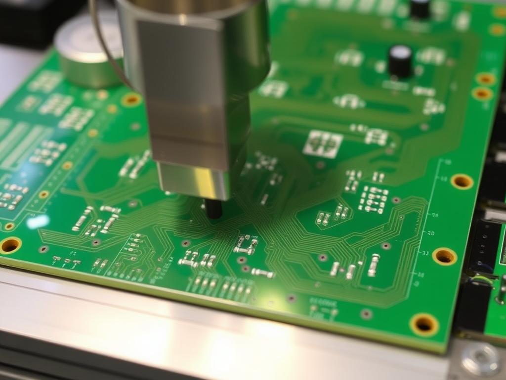
How Does Laser Depaneling Work and What are its Advantages?
Лазерное депанелирование has become my go-to for many complex projects. It’s a non-contact process that uses a high-powered laser beam to cut through the подложка печатной платы or base material. This means there’s minimal механическое напряжение на печатная плата, which is essential for sensitive components, especially in flex pcbs. The process is very precise. The laser melts, vaporizes, or ablates away the material, creating a clean cut along the separation line.
The advantages of the laser are numerous:
- Высокая точность: Лазерная резка allows for very intricate and precise cuts, making it ideal for flexible printed circuit boards and complex shapes. This is essential for high-density boards used in электронные устройства.
- Минимальный стресс: Unlike mechanical methods, there is no physical contact with the схема, which eliminates the risk of damage from physical forces and vibrations. This is particularly beneficial for sensitive гибкие схемы.
- Чистые разрезы: The heat generated by the laser melts the material in a controlled way, resulting in clean edges, reducing the need for additional cleaning. This is important for technical cleanliness of the final product.
- Гибкость: Лазерная технология can easily handle different materials and thicknesses by simply adjusting the laser settings. This flexibility is a major advantage when you are working with various board types.
- Автоматизация: Лазерные системы депанелирования can be easily integrated into automated production lines, leading to higher efficiency and reduced lead time.
- No Tooling: Unlike routing or punching, there is no need for custom fixtures for the laser depaneling process, which reduces setup time and costs, making it an excellent choice for small runs as well as larger production volumes.
I’ve personally witnessed how laser depaneling has made a massive difference in production for many of our clients. For instance, we had a client who had significant issues with damaged circuits when using a router. When they switched to laser depaneling, their production yield significantly improved, and their rework costs plummeted.
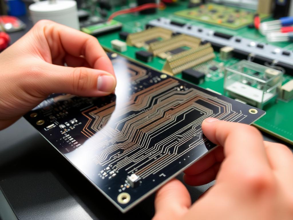
Why is Flexible PCB Depaneling a Unique Challenge?
Flexible printed circuit boards present a unique set of challenges in the depaneling process. Unlike the rigid pcbs, these flexible substrates are thin, delicate, and prone to tearing or deformation if not handled with the utmost care. The main problem lies in the flexible materials such as polyimide or polyethylene which are used as the base material.
Here’s why flex pcb depaneling plays an important role:
- Delicate Material: Flexible circuits can easily twist or bend, making it crucial to use a method that doesn’t apply excessive механическое напряжение. Traditional methods like v-groove or punching are simply not suitable.
- Complex Shapes: Гибкие печатные платы often come in complex shapes to fit into the final device. Traditional routing can be problematic with delicate and thin material and it can be challenging to precisely cut such shapes without causing damage.
- High Precision Requirements: Given the high density and compact nature of many flexible circuit applications, high precision is essential to avoid cutting into components and traces, especially for circuits that require conductive properties, such as circuits with exposed solder pads.
Because of these factors, laser depaneling is often the preferred method for flexible pcbs. The non-contact nature of the laser and its precision offer a solution that can handle the challenges of delicate materials and intricate designs without any problems. From my perspective, лазерная депанелизация has significantly improved the manufacturing process of flexible printed circuits, resulting in better quality and reduced scrap rates. This also enhances the whole process of flexible printed circuit производство.
What are the Key Advantages of Flexible Circuit Boards?
Over the years, I’ve seen the advent of new technologies push boundaries of what is possible with circuits and flexible printed circuits, and it’s amazing how these гибкие печатные платы have become an integral part of many электронные устройства. The most significant advantages are:
- Гибкость: This is the obvious advantage. The ability to bend, twist, and fold a circuit opens up many design possibilities. This is a very important factor in the modern electronic devices where devices are getting smaller and smaller.
- Space Saving: Гибкие печатные платы are much thinner than rigid pcbs, saving valuable space in electronic devices. That makes them ideal for compact applications like smartphones and wearable technology.
- Lightweight: These boards are also lighter than their rigid counterparts, which is crucial for portable электронные устройства. This can make a significant difference in wearable devices, pacemakers, and other devices where weight is a concern.
- Reliability: The absence of connectors and their associated failures can increase reliability in certain devices, because the circuits use проводящий materials that are directly printed or etched onto the flexible субстрат.
- Design Freedom: Гибкие печатные платы allow for more creative designs, such as circuits that can wrap around other components or fit into curved surfaces, and therefore, they are widely used in автомобильный, aerospace, and other specialized fields. This gives engineers a greater degree of freedom.
Гибкие печатные платы are a major advent in the electronics industry, enabling smaller, lighter, and more versatile electronic products. Their ability to adapt to complex shapes and reduce device footprints makes them a critical component in our modern world. I personally think it’s amazing how flexible circuits are also key components in applications like including smartphones, wearable devices, and even aerospace equipment, that shows the importance of such technology.
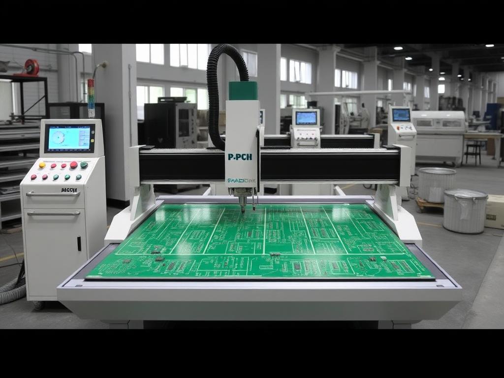
How Does a Router Fit into the PCB Cutting Process?
А маршрутизатор plays a significant role in the резка печатных плат и депанелирование process, especially for those who do not use laser depaneling. It uses a high-speed rotating milling cutter to cut through the печатная плата along predefined paths. The маршрутизатор cutting process is very precise, which is a good choice when handling complex shapes and cutouts.
Here’s what I’ve learned over my career about using routers in the процесс депанелирования:
- Универсальность: Routers can handle both rigid pcbs и flexible pcbs. By carefully controlling speed and depth of cut, you can achieve clean separation for different materials and thicknesses.
- Controllability: Modern routers offer programmable paths, which allows for complex shapes and cutouts, and very precise separation, so you have a high degree of control over the cutting процесс.
- Эффективность: With automation and in-line integration, routers can deliver decent throughput while maintaining the desired level of precision. This makes them viable for high production volumes.
- Экономически эффективно: Compared to lasers, router cutting machines can be more affordable. It is a great choice if you have larger production volumes and your circuits don’t have a lot of intricate designs.
- Limitations: Routing can induce a certain amount of механическое напряжение and vibration, which can damage delicate components and circuits. It can also generate dust, requiring a dust collection system to maintain technical cleanliness in the workplace.
While routers are a workhorse in many manufacturing facilities, from my experience, they’re not always the best choice for all situations, especially for very flexible and sensitive circuits.
What is the Role of Laser Technology in PCB Manufacturing?
Лазерная технология has revolutionized the Производство печатных плат process, especially in depaneling. The laser is very important because it provides a high-precision, non-contact way to cut and separate печатные платы. This technology is not limited to just cutting; it is used in a variety of pcb manufacturing steps.
I’ve seen first-hand how laser technology transforms many aspects of our workflow. Here are some of the applications where lasers are used:
- Депанеляция: As mentioned earlier, laser depaneling is a high-precision method that cuts through the board with minimal stress and is a good choice for both жесткий и flexible pcbs.
- Direct Imaging: Lasers can directly image the схемы на субстрат before etching, improving the accuracy of the медные слои and achieving the fine lines needed for high-density boards.
- Via Drilling: Lasers can create very small holes for vias, which are critical for connecting different медные слои in multi-layer boards. This is important in producing modern high-density boards.
- Marking and Tracking: Lasers are used for precision marking and tracking of boards, which is very useful in production and quality control. You can use lasers to create QR codes, serial numbers, and any other kind of marking for traceability.
- Flex PCB Fabrication: Лазерная резка is the most commonly used method for flexible pcbs. Lasers can handle the fragile material and create complicated designs on the flexible субстрат, and this is crucial in the manufacturing process of flexible printed circuit boards.
With laser’s capabilities like high-precision, flexibility, and minimal stress, I’ve come to rely on it for complex and sensitive circuit applications. It’s an invaluable tool for modern pcb manufacturing. For example, LPKF’s laser technology has been instrumental in the advent of new products.
What Are the Applications of Flexible Printed Circuit Boards?
Гибкие печатные платы are found in an incredible variety of applications, thanks to their unique flexibility, lightweight, and space-saving features. I’ve worked on projects where the applications of flexible pcbs are the backbone of the product, and they have transformed various industries.
Here are just some of the many uses for гибкие печатные платы:
- Smartphones: В smartphones and other handheld devices, flex pcbs connect various components in tight spaces, enabling thinner, lighter designs. They are used for connecting displays, cameras, and buttons, as they can fold and twist, and fit in the device’s tight spaces.
- Wearable Devices: In wearable technology, such as smartwatches and fitness trackers, the flexible nature of the circuits is essential for conforming to the human body. They are used in the heart rate sensors, display connections, and battery circuits.
- Автомобильная промышленность: Гибкие схемы are used in automotive applications such as dashboard controls, sensor connections, and lighting systems, due to their ability to withstand vibrations and temperature changes. They are also found in airbag sensors and camera systems.
- Медицинские приборы: They are used in pacemakers, hearing aids, and various monitoring devices where space and weight are critical. The flexibility and the reliability of the connections are essential for these applications.
- Аэрокосмическая промышленность: In aerospace, flex pcbs are used in avionics, satellite systems, and control panels, due to their lightweight nature and reliability.
- Бытовая электроника: You can also find гибкие печатные платы in digital cameras, laptops, and other devices, connecting the mainboard, screen, or other components, making these devices more compact and durable.
From my perspective, гибкие печатные платы have enabled innovation across numerous industries. Their unique properties offer design freedom and performance improvements that are impossible with rigid counterparts. The ability to conform to complex shapes allows the designers to create unique products.
Why is Technical Cleanliness Essential in the Depaneling Process?
In my many years of experience, I’ve seen how critical technical cleanliness is in the процесс депанелирования. The reason is simple: any kind of contamination in the circuits can lead to defects and reduce the long-term reliability of the final product.
Here’s why it is important in процесс депанелирования to keep everything clean:
- Contaminants: Dust, debris, and solder residues generated during the процесс депанелирования can settle on the boards, affecting solderability and electrical connections. These contaminants can cause short circuits or open circuits in the final product.
- Corrosion: If contaminants are left on the board, they can corrode the медные слои or other metal components, reducing the lifespan and reliability of the circuit.
- Electrical Conductivity: Contaminants can affect the dielectric properties and the conductive properties of the board, thus reducing performance, especially on high-density boards.
- Product Performance: The reliability of электронные устройства depends on the technical cleanliness. Any kind of contamination can reduce the long term stability and performance of the device.
- Quality Standards: Maintaining technical cleanliness ensures compliance with industry quality standards and customer requirements, and that will ensure less rework and less costs.
To achieve this high degree of technical cleanliness, the use of a proper ventilation system, and cleaning procedures, as well as avoiding dust generation by opting for laser depaneling can significantly reduce contamination. For me, keeping things clean is as important as the precision of cutting, and that is why we focus on providing clean solutions.
How Can You Contact Us to Find the Right Depaneling Solution?
After working in this field for so long, I understand the challenges you face when it comes to депанелирование печатной платы. Choosing the right equipment and method can be crucial to your project’s success, and we are here to help you.
If you’re looking for high-quality, efficient, and reliable depaneling solutions, please связаться с нами. Here is why you should get in touch:
- Экспертное руководство: We have over 20 years of experience in the field and offer expert advice to help you choose the best solution for your particular needs. I and my team have first-hand experience with different technologies.
- Wide Range of Solutions: We offer a wide range of depaneling machines, from simple routers to high-precision laser cutting systems and automatic equipment, and we can find you the right solution, no matter what your needs are.
- Индивидуальные решения: We provide custom solutions that fit your production requirements. If you have very specific requirements, we can tailor our products to meet those requirements.
- Industry Leaders: Our machines are used by many leading electronic companies, such as TP-LINK, Canon, BYD, Flex, TCL, Xiaomi, Lenovo, OPPO, HONOR, and Foxconn. This is a testament to the quality and reliability of our products.
- Постоянная поддержка: We offer ongoing support and maintenance to ensure that your machines perform efficiently and reliably over their lifespan.
- Автоматизация: Our automated solutions can significantly improve the speed and efficiency of your production line, reducing labor costs and improving throughput.
Don’t hesitate to reach out. Let’s discuss your specific needs, and we’ll help you find the perfect depaneling solution that fits your requirements. You can contact us here https://pcbdepaneling.com/contact-us/ and together we can make your production run smoothly.
Часто задаваемые вопросы
What are the main differences between laser depaneling and router cutting? Laser depaneling uses a laser beam for cutting and is very precise and has no mechanical stress, ideal for flexible circuits and intricate shapes, while router cutting uses a rotating blade, and although versatile is not as precise and can generate more stress and vibration.
Can laser depaneling be used for FR4 boards? Yes, laser depaneling can be used on FR4 boards, and it is a good solution if you have delicate components, tight tolerances and complex shapes. This approach will ensure that your product is high-quality.
Is it possible to automate the depaneling process? Yes, many depaneling machines, including laser and router systems, can be integrated into automated production lines for enhanced throughput and lower production costs.
What is the best method for depaneling flexible circuits? Laser depaneling is considered the best method due to its high precision and minimal mechanical stress, making it suitable for delicate flexible circuits.
What are the most important factors when selecting a depaneling method? The type of material, production volume, complexity of the circuit board, required precision, available budget and the needed technical cleanliness are important factors when deciding on your depaneling solution.
Ключевые выводы
- Depaneling is a critical step in PCB manufacturing that involves separating individual circuit boards from larger panels.
- Various depaneling methods exist, including V-groove, router cutting, punching, and laser cutting, each suited for different applications.
- Лазерное депанелирование is a high-precision, non-contact method ideal for complex and sensitive boards, especially flexible pcbs.
- Гибкие печатные платы present unique depaneling challenges due to their delicate nature and require careful handling and precise methods like лазерная резка.
- Maintaining technical cleanliness during the depaneling process is crucial to prevent contamination and ensure the reliability of the final product.
- Our wide range of depaneling solutions and expert guidance can help you choose the best approach for your needs. Машина для снятия панелей с нижней части печатной платы GAM 380AT is a great solution, but there are many more solutions for you to choose from.
- Гибкие печатные платы are crucial for modern devices due to their flexibility, space-saving design, and lightweight nature, especially for the smaller form factor devices.
- Лазерная технология is used in many PCB manufacturing processes, including depaneling, imaging, and drilling and has a very important role in modern PCB production.
- The Линейный автоматический фрезерный станок для печатных плат GAM 330AT is another great option for your production. If you do not want router, you can check our ZM30-ASV Полностью автоматическая пила для снятия панелей с V-образной канавкой решение.
I hope this comprehensive guide has given you valuable insights into the complex process of pcb depaneling. Remember, choosing the right method is critical for quality and efficiency of your production, and we are here to assist you in finding the perfect solution.
This is a very interesting topic, and if you would like to know more, you can check our Решение для линейной машины для разделения панелей SMT for an SMT production. And finally, if you are looking for laser solutions, you can also check our Лазерная депанельизация печатных плат page, where you can find the perfect solution for your needs.