![]()

Pros and cons of PCB router machines
Precision Perfected: Mastering PCB Milling and Routing for Flawless Circuit Boards
As someone who’s been in the trenches of pcb manufacturing for over two decades – as a ເຄື່ອງ PCB Router, ກ PCB Laser Depaneling expert, and even intimately familiar with the nuances of V-groove Depaneling, ເຄື່ອງເຈາະ PCB/FPC operations, and the integration of ອຸປະກອນອັດຕະໂນມັດ ແລະຈໍາເປັນ ອຸປະກອນເສີມ – I’ve seen firsthand the evolution of pcb mill technology. This isn’t just an article; it’s a deep dive born from years of experience, guiding you through the intricate world of router pcb ແລະ cnc machine technology to help you achieve impeccable ແຜ່ນວົງຈອນພິມ production. If you’re involved in ການອອກແບບ pcb, small cnc operations, or are exploring the best methods for milling pcbs or understanding the difference between milling ຫຼື routing, you’ve come to the right place. We’ll explore the critical questions and solutions, ensuring your journey in ແຜງວົງຈອນ ແລະ ວົງຈອນພິມ fabrication is smooth and successful.
Article Outline: Your Roadmap to PCB Milling Mastery
Here’s what we’ll be covering in this comprehensive guide to pcb milling and routing:
- ແມ່ນຫຍັງແທ້ a PCB Mill ຫຼື ເຄື່ອງ PCB Router and how does it differ from other cnc machine types?
- Why choose pcb milling process over traditional etch methods for your ແຜງວົງຈອນ?
- What are the key components of a router pcb and how do they impact pcb fabrication?
- How do you prepare your ການອອກແບບ pcb files (like ເກີເບີ files) for the ຂະບວນການ milling using software like FlatCAM?
- What considerations are crucial when selecting milling bit ແລະ ເຈາະ ສໍາລັບຂອງທ່ານ pcbs?
- How do you execute the pcb milling process, including setting feed rates ແລະ milling depth?
- What are the best practices for drilling drill holes and achieving accurate ຕັດຂອບ on your pcb board?
- What are the advantages of using a cnc machine for creating custom circuit boards compared to other fabrication ວິທີການ?
- From prototyping to production: When is pcb milling process the ideal solution for your ການຜະລິດ pcb needs?
- What future innovations are on the horizon for router pcb technology, and how can they benefit your pcb ປະກອບ process?
Delving into the World of PCB Milling and Routing
1. What exactly is a PCB Mill ຫຼື ເຄື່ອງ PCB Router and how does it differ from other cnc machine types?
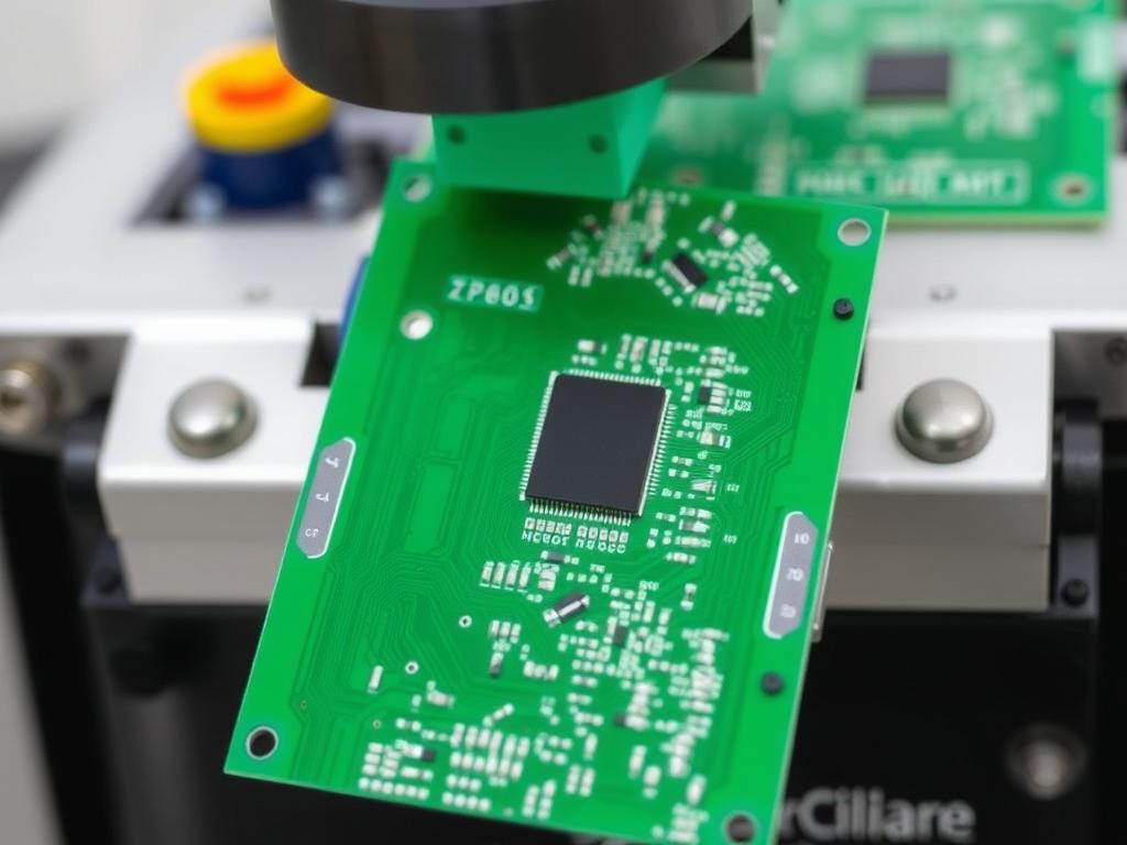
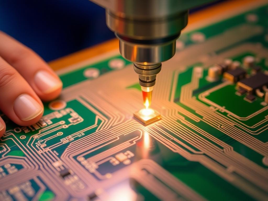
As a ເຄື່ອງ PCB Router, I can tell you firsthand that my primary function is the precise removal of material from a pcb board to create the desired electrical circuits. Think of it as a specialized cnc machine meticulously carving out the conductive pathways, isolating pads, and shaping the board’s edges. While sharing the core principles of cnc machining – controlled movement along multiple axes (x and y axes, and often a z ແກນ) guided by computer numerical control (cnc) – a pcb mill is specifically designed for the delicate work required for ແຜງວົງຈອນພິມ. Unlike general-purpose milling machines that might work with metal or wood, our focus is on materials like FR4, copper, and sometimes flexible substrates. This often involves higher spindle speeds and finer ຄວາມທົນທານ capabilities to accurately create the intricate traces and pads essential for modern electronics.
2. Why choose pcb milling process over traditional etch methods for your ແຜງວົງຈອນ?
Having witnessed the evolution of pcb fabrication, I can confidently say that pcb milling process offers compelling advantages, especially for prototyping and low-volume production. Traditional etch methods involve chemical etching, using etchants like ferric chloride or ammonium persulfate ກັບ remove copper. While effective for ການຜະລິດຈໍານວນຫລາຍ, this process can be time-consuming, involve hazardous chemicals, and require careful disposal. In contrast, milling provides a faster turnaround for design iterations. As a ເຄື່ອງເຈາະ PCB/FPC and having seen the precision offered by PCB Laser Depaneling, I appreciate the clean, dry process of milling, which avoids the mess and environmental concerns of chemical etch. It’s also ideal for creating double sided boards and even intricate multi-layer designs without the complexities of chemical registration. For those who need a pcb quickly to test a board design, milling provides that agility.
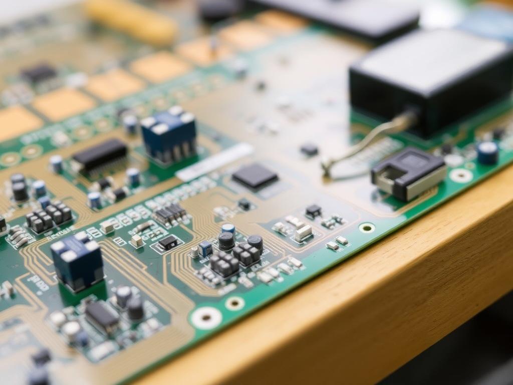
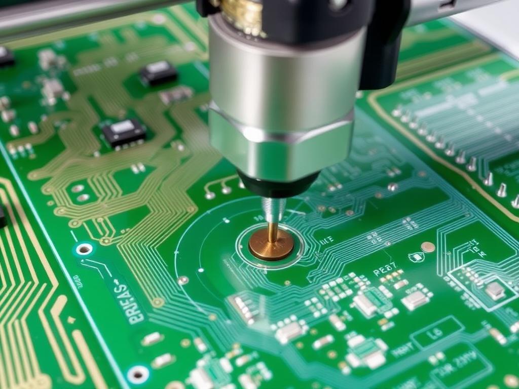
3. What are the key components of a router pcb and how do they impact pcb fabrication?
As a ເຄື່ອງ PCB Router, my core lies in several key components working in harmony. The high-speed spindle is the heart, holding the milling bit ຫຼື ເຈາະ and spinning it at thousands of RPMs to precisely ຕັດ ໄດ້ copper layer. ໄດ້ gantry system, often utilizing precise linear bearing ແລະ ball bearings, ensures smooth and accurate movement of the spindle across the pcb board. A robust ຍຶດ system is vital to securely hold the ຊັ້ນໃຕ້ດິນ ໃນລະຫວ່າງ milling operation, preventing unwanted movement that could compromise accuracy. The cnc firmware interprets the design files and directs the stepper motor controlling the gantry’s movement. Effective ການສະກັດເອົາຂີ້ຝຸ່ນ is also a crucial, often overlooked, component for maintaining a clean work environment and ensuring clear visibility during the ຂະບວນການ milling. Each of these elements contributes to the final quality and precision of the ເສັ້ນທາງ pcb.
4. How do you prepare your ການອອກແບບ pcb files (like ເກີເບີ files) for the ຂະບວນການ milling using software like FlatCAM?
The journey from ການອອກແບບ pcb to physical board requires translating your design into instructions a cnc machine can understand. ເກີເບີ files, the industry standard for pcb layout information, need to be processed by software like FlatCAM. FlatCAM allows you to import your ເກີເບີ files and your drill file, representing the conductive layers, solder mask, and drill locations. You then define the ເຄື່ອງມືຕັດ parameters, such as the diameter of the hole for drilling or the end mill size for routing. FlatCAM generates the milling paths or G-code, the numerical control language that guides the cnc machine. It’s crucial to accurately specify parameters like milling depth ແລະ milling depth per single pass to achieve the desired results and avoid damaging the ຊັ້ນໃຕ້ດິນ ຫຼື ເຄື່ອງມືຕັດ. Understanding software like ກິກາດ ສໍາລັບ ການອອກແບບ pcb and its compatibility with FlatCAM is essential for a seamless workflow.
5. What considerations are crucial when selecting milling bit ແລະ ເຈາະ ສໍາລັບຂອງທ່ານ pcbs?
ການເລືອກທີ່ຖືກຕ້ອງ ເຄື່ອງມືຕັດ is paramount for achieving good results ໃນ pcb work. As someone intimately familiar with the ອຸປະກອນເສີມ side of things, I can emphasize the importance of material, geometry, and size. For isolating traces and pads, small diameter milling bits are used, often carbide for durability. V-carve bits are excellent for creating isolation channels. For drill holes, selecting the correct ເຈາະ size based on the ຜ່ານ and component lead sizes is crucial. High-speed steel (HSS) bits are suitable for some materials, but carbide bits offer superior lifespan and performance, especially for finer holes. Consider the copper layer thickness and the ຊັ້ນໃຕ້ດິນ material when selecting your bits. Using the wrong bit can lead to broken bits, poor cut quality, or damage to the pcb board.
6. How do you execute the pcb milling process, including setting feed rates ແລະ milling depth?
The execution phase requires careful attention to detail. Securely ຍຶດ ໄດ້ pcb board ໃສ່ ເຄື່ອງ bed. Load the generated G-code into the cnc controller. Setting the feed rates (the speed at which the ເຄື່ອງມືຕັດ moves across the material) and milling depth (how deep the ເຄື່ອງມືຕັດ cuts in each pass) are critical parameters. Too high a feed rate can cause the bit to break or chip the pcb board, while too low a rate can lead to excessive heat and wear on the bit. Similarly, the milling depth per pass needs to be appropriate for the material and ເຄື່ອງມືຕັດ. Often, multiple passes at shallower depths are preferable to a deep single pass, especially for thicker copper or delicate structures. Always perform a test run on a scrap piece if you are unsure of the optimal settings.
7. What are the best practices for drilling drill holes and achieving accurate ຕັດຂອບ on your pcb board?
ຂຸດເຈາະ small holes accurately requires a stable ເຄື່ອງ, sharp ເຈາະs, and appropriate feed rates. Ensure your ເຈາະ is securely chucked and running true. For ຕັດຂອບ, which defines the final shape of your pcb board, ແຂງແຮງ end mill designed for side-cutting is recommended. Program the milling paths for the ຕັດຂອບ carefully, often using an “outline” strategy. Consider leaving small tabs to hold the board in place during the ຂະບວນການ milling, which can be broken or cut away afterwards. Accurate ຕັດຂອບ is crucial for proper fitment in enclosures and for a professional finish. As a V-groove Depaneling expert, I understand the importance of clean and precise separation, and the same principles apply to ຕັດຂອບ ການນໍາໃຊ້ a ເຣົາເຕີ.
8. What are the advantages of using a cnc machine for creating custom circuit boards compared to other fabrication ວິທີການ?
As someone involved in various ການຜະລິດ pcb processes, including ອຸປະກອນອັດຕະໂນມັດ for handling and sorting, I see the distinct advantages of cnc milling for custom circuit boards. The speed and convenience for prototyping are unparalleled. You can go from design to a physical board in a matter of hours. The ability to easily iterate on designs without the delays and costs associated with chemical processing is a significant benefit, especially for hobbyists and small businesses. Furthermore, milling provides greater control over the ຂະບວນການ milling, allowing for intricate designs and the creation of features that might be difficult or impossible with chemical etching. For low to medium volume production, pcb milling offers a cost-effective and efficient solution.
9. From prototyping to production: When is pcb milling process the ideal solution for your ການຜະລິດ pcb needs?
ໃນຂະນະທີ່ chemical etching remains the dominant method for ການຜະລິດຈໍານວນຫລາຍ, pcb milling process shines in specific scenarios. For rapid prototyping and testing new ການອອກແບບ pcb concepts, milling provides an immediate feedback loop. For small production runs or custom circuit boards where flexibility and quick turnaround are paramount, it’s an excellent choice. Educational institutions and research labs often prefer milling due to its ease of use and safety compared to chemicals. If your designs require intricate features or you’re working with specialized materials where chemical processing is challenging, pcb milling would be a better fit. However, for very high-volume production, the scalability and cost-effectiveness of ຂະບວນການ etching generally outweigh the benefits of milling.
10. What future innovations are on the horizon for router pcb technology, and how can they benefit your pcb ປະກອບ process?
ພາກສະຫນາມຂອງ router pcb technology is constantly evolving. We’re seeing advancements in spindle technology leading to higher speeds and improved precision. Integration with robotic arms and automated material handling systems, much like our ອຸປະກອນອັດຕະໂນມັດ, is streamlining the entire pcb ປະກອບ process. Improved cnc firmware and software are making the programming and operation of these machines use easier and more intuitive. Developments in multi-axis cnc machines allow for more complex 3D milling ຫຼື routing ຂອງ ແຜງວົງຈອນ. These innovations will lead to faster turnaround times, increased automation, and the ability to create even more sophisticated and compact electronic devices. Even the integration of PCB Laser Depaneling technology into hybrid systems could offer even greater flexibility in ການຜະລິດ pcb.
FAQs: Your Burning PCB Milling Questions Answered
ຂໍ້ໄດ້ປຽບຕົ້ນຕໍຂອງການນໍາໃຊ້ a pcb mill? The primary benefits include rapid prototyping, no harsh chemicals, ease of iteration, and the ability to create complex geometries.
ແມ່ນ pcb milling suitable for double-sided PCBs? Yes, with careful alignment and fixturing, double sided PCBs can be effectively milled.
What software is commonly used for generating G-code for pcb milling? FlatCAM is a popular open-source option, but other commercial software packages are also available.
How accurate are pcb milling machines? Modern pcb milling machines can achieve very high accuracy, often down to a few thousandths of an inch, depending on the ເຄື່ອງ and settings.
Can a pcb mill also be used for pcb drilling? Yes, most pcb mills are equipped with a spindle capable of holding ເຈາະs for creating drill holes.
Key Takeaways: Mastering the Art of PCB Milling
- PCB milling is a versatile method for creating ແຜງວົງຈອນ, especially for prototyping and low-volume production.
- Understanding the components of a router pcb and their functions is crucial for successful pcb fabrication.
- Proper file preparation using software like FlatCAM is essential for generating accurate milling paths.
- Selecting the correct milling bit ແລະ ເຈາະ is critical for achieving quality results.
- Careful execution, including setting appropriate feed rates ແລະ milling depth, is vital for preventing errors.
- PCB milling provides significant advantages over traditional etching for rapid prototyping and custom circuit boards.
- Future innovations in router pcb technology promise even greater efficiency and capabilities.
Ready to revolutionize your ການຜະລິດ pcb? As a leading manufacturer of ເຄື່ອງ PCB Router, PCB Laser Depaneling, ແລະ V-groove Depaneling solutions, we have the expertise and technology to meet your needs. Our products are trusted by industry giants like TP-LINK, Canon, BYD, Flex, TCL, Xiaomi, Lenovo, OPPO, HONOR, and Foxconn. Contact us today to explore how our advanced depaneling and milling solutions can elevate your electronic manufacturing processes. Let’s build the future of electronics together!
Learn more about our PCB Router Machines Explore our advanced PCB Laser Depaneling solutions Discover our precise V-Groove Depaneling options See our range of efficient PCB/FPC Punching Machines Automate your production with our Automatic Equipment Find the right Accessories for your depaneling needs