![]()

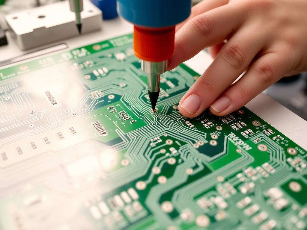
Ceramic PCB depaneling
Precision PCB & Ceramic Laser Depaneling: Achieving Flawless Separation
For over two decades, I’ve witnessed firsthand the evolution of PCB depaneling. From the early days of manual methods to the sophisticated laser technology we employ today, the goal remains the same: cleanly and efficiently separating individual pcb units from larger pcb panels. This article delves into the world of laser depaneling, specifically for both standard pcb materials and the increasingly important ceramic pcb. It’s a must-read for electronic technology companies, large processing factories, and even individual pcb enthusiasts seeking the most advanced and reliable ວິທີການ depaneling. We’ll explore why depaneling with lasers has become the gold standard and how it can benefit your operations, drawing upon my 20 years of experience in this dynamic field.
Article Outline: Mastering PCB & Ceramic Laser Depaneling
Here’s a roadmap of what we’ll cover, exploring the nuances of laser depaneling and its benefits for both traditional and ceramic pcb applications:
What Makes Laser Depaneling the Premier PCB Separation Method?
Why is Laser Cutting the Superior Choice for Ceramic PCBs?
How Does Laser Depaneling Minimize Mechanical Stress on Sensitive Circuits?
What are the Key Advantages of Using Laser Depaneling for High-Precision Applications?
Can Laser Depaneling Handle Complex PCB Geometries and Materials?
Is Laser Depaneling a Cost-Effective Solution Compared to Traditional Methods?
What Types of Ceramic PCBs Benefit Most from Laser Depaneling?
How Does Our Experience in PCB Router Machines Translate to Laser Excellence?
What Should You Consider When Choosing a Laser Depaneling Solution?
Ready to Optimize Your Depaneling Process with Advanced Laser Technology? Contact Us!
What Makes Laser Depaneling the Premier PCB Separation Method?
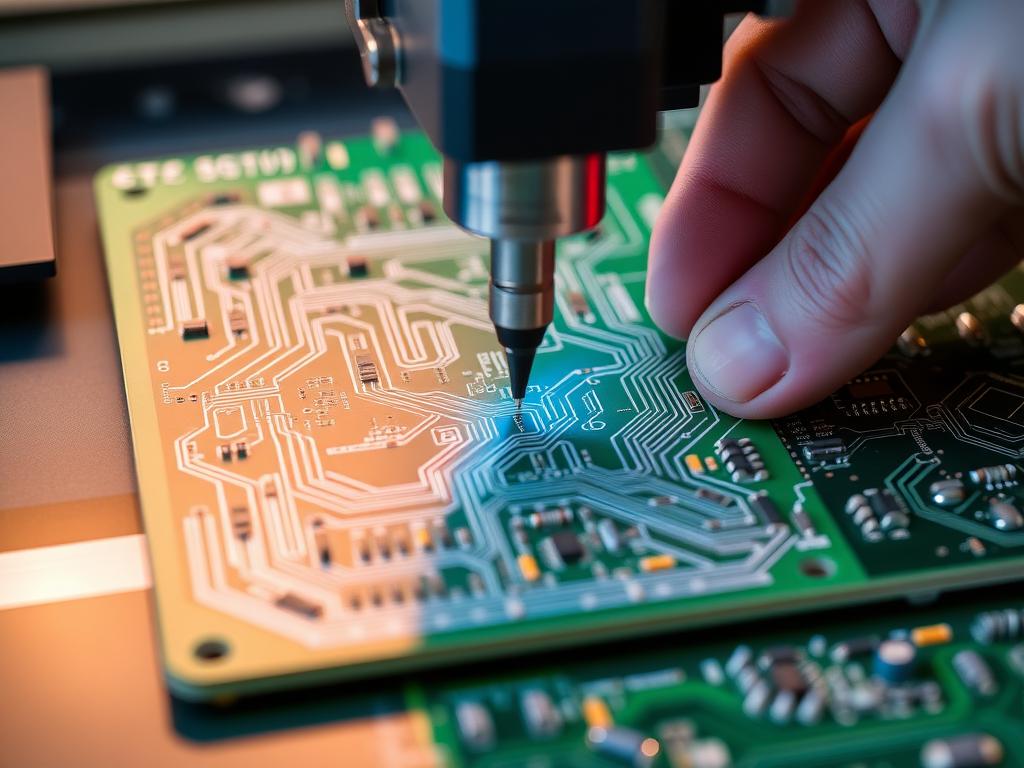
Having spent years observing and implementing various ການຍົກເລີກ techniques, I can confidently say that laser depaneling ໄດ້ປະຕິວັດວິທີທີ່ພວກເຮົາແຍກ ແຜງວົງຈອນພິມ. Unlike traditional methods that rely on physical force, ເລເຊີ technology offers a ບໍ່ຕິດຕໍ່ approach. This is a game-changer, especially when dealing with densely populated pcb panels. Think about it: a traditional ເຣົາເຕີ bit applies pressure, potentially causing ຄວາມກົດດັນກົນຈັກ that can damage delicate components or circuit traces. ເລເຊີ depaneling, on the other hand, utilizes a highly focused ເລເຊີ to precisely ablate the material along the separation lines. This means cleaner cut edges, reduced dust and debris, and significantly less ຄວາມກົດດັນໃນຄະນະ. ສໍາລັບ multilayer pcbs and those with intricate designs, the ຄວາມຊັດເຈນ offered by a laser system is unparalleled. We’ve seen firsthand how this translates to higher yields and improved product reliability for our customers.
The inherent flexibility of laser depaneling also stands out. With a ເຣົາເຕີ, you’re limited by the shape and size of the ເຄື່ອງມື. ການຕັດເລເຊີ, however, can handle complex contours and intricate patterns with ease. Imagine needing to separate a uniquely shaped pcb with tight tolerances. A traditional ວິທີການຕັດ might struggle, but a ເລເຊີ can navigate those curves with remarkable accuracy. This versatility extends to different pcb materials as well. Whether it’s standard FR-4 or more specialized substrates, the ລະບົບ laser depaneling can be adjusted to achieve optimal results.
Why is Laser Cutting the Superior Choice for Ceramic PCBs?
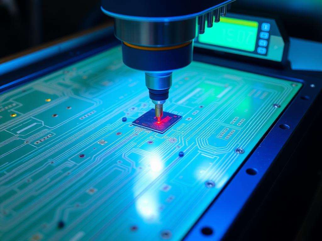
The rise of ceramic pcbs in high-performance applications like automotive sensors and high-frequency electronics has brought new challenges to the ການຍົກເລີກ ຂະບວນການ. Ceramic materials are inherently brittle and susceptible to cracking or chipping under ຄວາມກົດດັນກົນຈັກ. This is where ຕັດເລເຊີ truly shines. Traditional methods like die cutting or even specialized ceramic circuit board depaneling tools often introduce unacceptable levels of ຄວາມກົດດັນກົນຈັກ, leading to microfractures and compromised ຄວາມຫນ້າເຊື່ອຖື.
ກັບ laser depaneling, ໄດ້ ບໍ່ຕິດຕໍ່ nature of the process eliminates these risks. The focused ເລເຊີ creates a clean separation without putting undue pressure on the delicate ceramic substrate. This is critical for maintaining the structural integrity and electrical performance of ceramic circuit boards. We’ve seen instances where customers struggled with traditional methods, experiencing significant yield losses due to cracking. Switching to laser depaneling completely resolved these issues, demonstrating the technology’s unique suitability for ceramic pcbs. ໄດ້ ຄວາມຊັດເຈນ ຂອງ ເລເຊີ also allows for intricate cuts and complex shapes, which is often required in compact ceramic pcb ການອອກແບບ.
How Does Laser Depaneling Minimize Mechanical Stress on Sensitive Circuits?
As I mentioned earlier, the primary advantage of laser depaneling lies in its ບໍ່ຕິດຕໍ່ nature. Think of trying to separate individual stamps from a sheet. You could try to tear them apart, risking damage, or you could carefully cut along the perforations. ການຕັດກົນຈັກ methods are akin to tearing, while laser depaneling is like making those precise cuts. Methods like using a ເຣົາເຕີ ຫຼື ກ ດີໃຈຫລາຍ inherently involve physical force. This force can translate to vibration ແລະ ຄວາມກົດດັນໃນຄະນະ, potentially damaging sensitive components, especially those near the edges of the pcb. For high-density smt assembly, even microscopic damage can lead to failures down the line.
ເລເຊີ depaneling, utilizing a focused ເລເຊີ, essentially melts or vaporizes the material along the intended separation lines. ນີ້ ablation process is incredibly localized, meaning the heat-affected zone is minimal, further reducing any thermal ຄວາມກົດດັນ. The result is a clean break with minimal ຄວາມກົດດັນກົນຈັກ, ensuring the integrity of the ວົງຈອນ. This is particularly crucial for applications where ຄວາມຫນ້າເຊື່ອຖືສູງ is paramount, such as in medical devices or aerospace electronics. We’ve seen companies significantly reduce their failure rates after adopting laser depaneling, a testament to its gentle yet effective approach.
What are the Key Advantages of Using Laser Depaneling for High-Precision Applications?
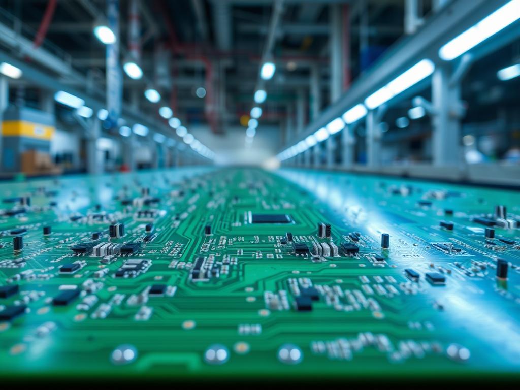
In the world of electronics manufacturing, ຄວາມຊັດເຈນ is paramount. Whether you’re dealing with intricate circuit traces on a standard pcb or the fine features of a ceramic pcb, accurate ການຍົກເລີກ ເປັນສິ່ງຈໍາເປັນ. ເລເຊີ depaneling offers a level of ຄວາມຊັດເຈນ that traditional methods simply can’t match. The focused ເລເຊີ, often with a beam diameter of just a few microns, allows for incredibly fine and accurate cuts. This is crucial for maintaining tight tolerances and ensuring proper functionality of the ຍົກເລີກ ກະດານ.
Consider the separation of densely populated ແຜງ pcb. ກ ເຣົາເຕີ bit, even a small one, has a physical width that can encroach on valuable board space. With laser depaneling, the narrow ເລເຊີ can navigate closely spaced components without causing interference. This is particularly important for miniaturized electronics where every millimeter counts. Furthermore, the ຄວາມແມ່ນຍໍາສູງ ຂອງ ເລເຊີ translates to cleaner cut edges, minimizing the need for post-processing and improving the overall aesthetic quality of the final product. This ຄວາມແມ່ນຍໍາສູງ also extends to the ability to create complex shapes and internal cutouts that would be difficult or impossible with other ລະບົບ depaneling.
Can Laser Depaneling Handle Complex PCB Geometries and Materials?
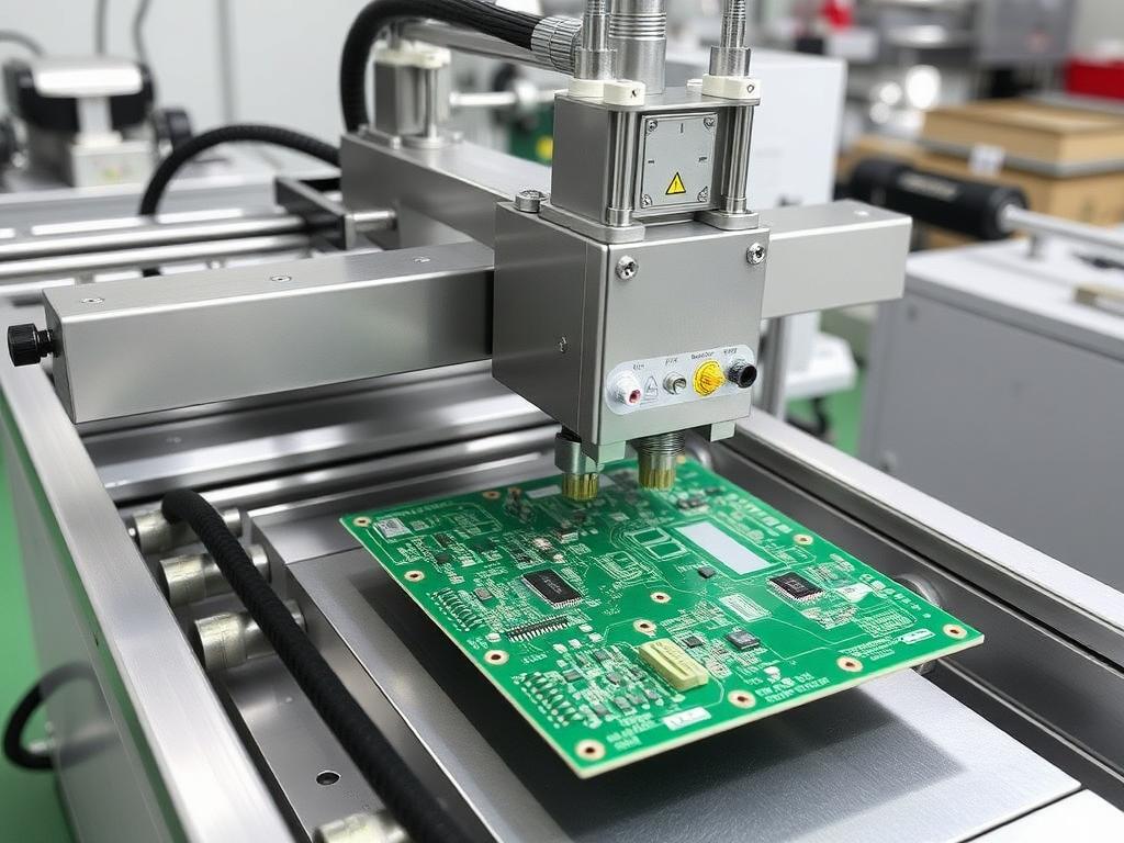
The versatility of laser depaneling is one of its key strengths. Unlike mechanical methods that are often limited by the geometry of the ເຄື່ອງຕັດ or the force applied by a ດີໃຈຫລາຍ, ກ ເລເຊີ can adapt to virtually any shape and material. Think about separating pcbs with curved edges, intricate tabs, or internal cutouts. These complex geometries can be challenging for traditional ເຄື່ອງຈັກ depaneling. However, the programmable nature of a laser system allows it to follow complex paths with ease, delivering clean and accurate ຕັດທີ່ຊັດເຈນ every time.
Beyond geometry, laser depaneling also excels at handling a wide range of materials. While it’s particularly well-suited for the brittle nature of ceramic pcbs, it can also effectively depanel standard FR-4, flex pcbs, and even metal-core pcbs. The key is adjusting the ເລເຊີ parameters – power, speed, and frequency – to optimize the ຂະບວນການຕັດ for the specific material. This adaptability makes laser depaneling a future-proof solution for manufacturers who work with diverse pcb types. We’ve helped numerous clients transition from struggling with challenging materials using mechanical methods to achieving seamless ແຍກ ກັບ lasers.
Is Laser Depaneling a Cost-Effective Solution Compared to Traditional Methods?
While the initial investment for a ລະບົບ laser depaneling might seem higher than for a simple ເຣົາເຕີ ຫຼື ດີໃຈຫລາຍ, a closer look at the overall cost of ownership reveals significant long-term savings. Consider the factors beyond the initial purchase price. ເລເຊີ depaneling eliminates the need for costly and frequently replaced cutting tools like ໂຮງສີ bits. The ບໍ່ຕິດຕໍ່ nature of the process also reduces the risk of damaging pcbs, leading to fewer scrapped boards and higher yields. This is especially true for delicate ceramic circuit boards where a single cracked board can represent a significant loss.
ນອກຈາກນັ້ນ, laser depaneling often requires less manual intervention, especially when integrated with ອັດຕະໂນມັດ systems. This translates to lower labor costs and increased ຜ່ານ. ໄດ້ ຄວາມຊັດເຈນ and clean cut edges produced by lasers can also minimize the need for secondary finishing processes, further reducing costs and cycle time. While methods like v-groove depaneling might seem like a lower cost option upfront, they often lack the flexibility and ຄວາມຊັດເຈນ ຂອງ laser depaneling, potentially leading to higher costs down the line due to rework or lower quality. In the long run, the increased efficiency, reduced waste, and improved quality offered by laser depaneling make it a highly ຄ່າໃຊ້ຈ່າຍປະສິດທິພາບ ການແກ້ໄຂ.
What Types of Ceramic PCBs Benefit Most from Laser Depaneling?
The unique properties of ceramic pcbs make them ideal for demanding applications requiring high thermal conductivity, excellent electrical insulation, and robust performance in harsh environments. However, their brittleness makes traditional ວິທີການ depaneling a significant challenge. Almost all types of ceramic pcbs stand to benefit from the precision and minimal ຄວາມກົດດັນກົນຈັກ ສະເໜີໂດຍ laser depaneling.
This includes:
- Alumina PCBs: Commonly used in power electronics and high-temperature applications.
- Aluminum Nitride PCBs: Offering even higher thermal conductivity, ideal for LED lighting and RF applications.
- Beryllium Oxide PCBs: Known for exceptional thermal conductivity, used in high-power microwave applications.
For all these ceramic pcb types, laser depaneling ensures clean ແຍກ without cracking or chipping, maintaining their critical performance characteristics. Whether it’s a simple rectangular ceramic circuit board or one with complex shapes and internal features, ຕັດເລເຊີ provides the necessary accuracy and control. The ability to create intricate separation lines is particularly beneficial for high-density ceramic pcbs used in compact electronic devices.
How Does Our Experience in PCB Router Machines Translate to Laser Excellence?
ໃນຂະນະທີ່ laser depaneling represents the cutting edge of the technology, our deep roots in ເຄື່ອງ router pcb manufacturing provide a crucial foundation for our expertise in ເລເຊີ solutions. For years, we’ve been at the forefront of understanding the intricacies of pcb materials, the mechanics of ການຍົກເລີກ, and the importance of ຄວາມຊັດເຈນ in the manufacturing process. This extensive experience with ເຣົາເຕີ technology gives us a unique perspective when designing and implementing ລະບົບ laser depaneling.
We understand the nuances of different ວິທີການ depaneling, their strengths, and their limitations. This allows us to offer informed guidance to our customers, helping them choose the optimal solution for their specific needs. Our experience in building robust and reliable ເຄື່ອງ router pcb also translates to the quality and durability of our ລະບົບ laser depaneling. We leverage our engineering expertise to create machines that are not only precise but also built to withstand the demands of continuous industrial operation. Essentially, our history in ເຣົາເຕີ technology provides a comprehensive understanding of the ການຍົກເລີກ landscape, allowing us to excel in the realm of ເລເຊີ ວິທີແກ້ໄຂ.
What Should You Consider When Choosing a Laser Depaneling Solution?
ການເລືອກສິດ ລະບົບ laser depaneling is a crucial decision that can significantly impact your manufacturing efficiency and product quality. Several key factors should be considered:
- ຄວາມເຂົ້າກັນໄດ້ຂອງວັດສະດຸ: ຮັບປະກັນ laser system is capable of effectively depaneling the specific pcb materials you use, including both standard and ceramic materials.
- Precision and Accuracy: ປະເມີນຜົນ laser’s ability to achieve the required tolerances and create clean cut edges for your applications. Consider the ເລເຊີ size and positioning accuracy.
- Throughput Requirements: ປະເມີນ ການຍົກເລີກ speed and automation capabilities of the system to meet your production volume needs. Higher ຜ່ານ translates to greater efficiency.
- ຊອບແວ ແລະການຄວບຄຸມ: Look for intuitive software that allows for easy programming of ຕັດ paths and integration with your existing manufacturing systems.
- ການບໍາລຸງຮັກສາແລະສະຫນັບສະຫນູນ: Consider the availability of reliable technical support and readily available spare parts to minimize downtime.
- Cost of Ownership: Analyze the total cost, including initial investment, operating costs (power consumption, consumables), and maintenance.
- ຄຸນນະສົມບັດຄວາມປອດໄພ: ຮັບປະກັນ laser system incorporates appropriate safety measures to protect operators.
By carefully evaluating these factors, you can choose a laser depaneling solution that perfectly aligns with your specific requirements and delivers long-term value.
Ready to Optimize Your Depaneling Process with Advanced Laser Technology? Contact Us!
After 20 years in the pcb industry, witnessing the evolution of ການຍົກເລີກ from manual separation to the incredible ຄວາມຊັດເຈນ ຂອງ ເລເຊີ technology, I’m genuinely excited about the possibilities that laser depaneling offers. Whether you’re working with standard pcbs or the demanding requirements of ceramic pcbs, the benefits are undeniable: reduced ຄວາມກົດດັນກົນຈັກ, unparalleled ຄວາມຊັດເຈນ, increased efficiency, and improved product ຄວາມຫນ້າເຊື່ອຖື. ຂອງພວກເຮົາ ລະບົບ laser depaneling are trusted by industry leaders like TP-LINK, Canon, BYD, Flex, TCL, Xiaomi, Lenovo, OPPO, HONOR, and Foxconn – companies that demand the highest quality and performance.
Don’t let outdated ວິທີການ depaneling hold you back. ຕິດຕໍ່ພວກເຮົາ today to discuss your specific needs and discover how our advanced ເຕັກໂນໂລຊີ laser ສາມາດຫັນປ່ຽນຂອງທ່ານ pcb manufacturing process. Let’s explore how we can help you achieve flawless ແຍກ, minimize waste, and maximize the ຄວາມຫນ້າເຊື່ອຖື of your products. We’re here to guide you through the transition and ensure you’re leveraging the full potential of laser depaneling.
FAQs:
ປົກກະຕິແມ່ນຫຍັງ ຄວາມຫນາ range that laser depaneling can handle? Laser depaneling can handle a wide range of thicknesses, typically from very thin flexible circuits up to several millimeters, depending on the material and laser power.
Does laser depaneling create a lot of residual dust or debris? Compared to mechanical methods, laser depaneling produces significantly less residual material. Any minimal debris is usually very fine and can be easily managed with proper extraction systems.
ແມ່ນ laser depaneling suitable for high-volume production? Yes, ລະບົບ laser depaneling can be highly automated and offer high ຜ່ານ, making them well-suited for high-volume production environments.
ປະເພດຂອງການບໍາລຸງຮັກສາແມ່ນຕ້ອງການສໍາລັບການ ລະບົບ laser depaneling? Maintenance typically involves cleaning optical components, checking cooling systems (water cooling is common), and occasional replacement of consumable parts.
ແນວໃດ laser depaneling ensure technical cleanliness? The non-contact nature and minimal debris generation of laser depaneling contribute to excellent technical cleanliness, which is crucial for many electronic applications.
Summary of Key Takeaways:
- ເລເຊີ depaneling offers superior ຄວາມຊັດເຈນ and minimizes ຄວາມກົດດັນກົນຈັກ compared to traditional methods.
- It is the ideal solution for depaneling brittle materials like ceramic pcbs.
- ການຕັດເລເຊີ can handle complex geometries and a wide range of pcb ວັດສະດຸ.
- While the initial investment may be higher, laser depaneling offers long-term ຄ່າໃຊ້ຈ່າຍປະສິດທິພາບ through reduced waste and increased efficiency.
- Our extensive experience in ເຄື່ອງ router pcb provides a solid foundation for our expertise in laser depaneling.
- Careful consideration of material compatibility, ຄວາມຊັດເຈນ, ຜ່ານ, and other factors is crucial when choosing a ລະບົບ laser depaneling.
ການເຊື່ອມຕໍ່ພາຍໃນ:
- Learn more about our versatile ເຄື່ອງ PCB Router.
- Explore our advanced solutions for V-groove Depaneling.
- See our offerings for ເຄື່ອງເຈາະ PCB/FPC.
- ຄົ້ນພົບຂອງພວກເຮົາ ອຸປະກອນອັດຕະໂນມັດ for streamlining your production line.
- View our range of essential ອຸປະກອນເສີມ.
- ສຳຫຼວດຄວາມສົມບູນຂອງພວກເຮົາ SMT ອຸປະກອນສາຍທັງຫມົດ ວິທີແກ້ໄຂ.