![]()

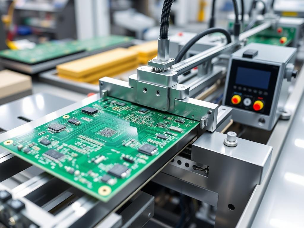
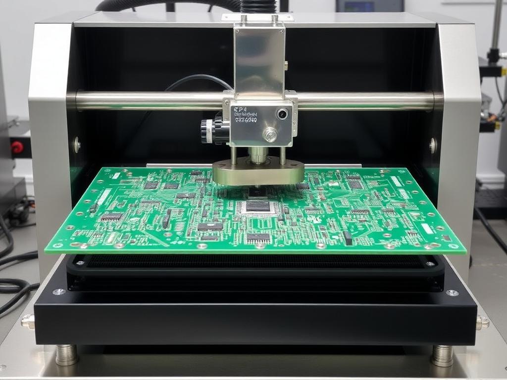
PCB depaneling system for mass production
Precision PCB Depaneling: Choosing the Right Method for Your Production Line
As someone deeply embedded in the world of 인쇄 회로 기판 manufacturing for the past two decades, I’ve witnessed firsthand the evolution of 디패널링 – the critical process of separating individual 인쇄 회로 기판 더 큰 것에서 패널. This article isn’t just another dry technical overview; it’s a journey through the various methods of PCB depaneling, sharing my practical experiences and insights to help you make the best choices for your 제조 공정. We’ll explore everything from traditional 라우팅 to advanced 레이저 디패널링, ensuring you understand how to achieve optimal results for your specific needs. From TP-LINK to Foxconn, the world’s biggest electronics giants choose us – and I’m here to show you why.
The Crucial Role of Depaneling in PCB Production
Okay, let’s get down to it. The 디패널링 process, also sometimes called singulation, is essential. Once the 인쇄 회로 기판 are populated with their electronic components, the large pcb panel is no longer needed, and the individual 회로 must be separated. But how is this done? Well, there are several 디패널링 방법 available, each with their own advantages and disadvantages. The right choice of method isn’t just about separating boards; it’s about maintaining the integrity of the 회로 and ensuring the efficient operation of your 생산라인. Do you know which 디패널링 approach best fits your production needs? This article aims to answer exactly that.
Understanding Your PCB Depaneling Needs
Before we dive into the specific 디패널링 방법, it’s critical to understand what factors influence your decision. Are you dealing with rigid pcbs 또는 flex pcbs? What is the height of the components? What type of pcb are you working with? Do you need 인라인 디패널링 to increase production line speed or is an offline solution better for your workflow? The answers to these questions will significantly influence the type of 디패널링 기계 you should consider. Also, is cleanliness a critical concern? How about 기계적 응력? It’s all part of the equation.
What Are the Different Types of PCB Depaneling Methods?
There’s more than one way to separate 개별 pcb. Each method has unique characteristics, and the right one depends on your requirements. What works for a small batch of simple boards won’t cut it for high-volume, complex assemblies. As we move on, we’ll cover each method in detail, including the pros, the cons, and the appropriate applications.
Mechanical Routing: The Workhorse of PCB Separation
Mechanical 라우팅, using a 라우터, is a widely used method that involves using a specialized cutting 도구 to mill the 피씨비 material along a predefined path. This is suitable for various types of pcbs, offering good precision and versatility. However, it also has limitations with its speed and can leave behind some dust and debris. But it’s still a solid, 비용 효율적 option for many pcb 제조 operations.
V-Groove Depaneling: Efficient for Straight Lines
V형 홈 depaneling, also known as v-점수, utilizes a blade with a V-shaped profile to create a channel on both sides of the pcb panel, allowing the boards to be snapped apart. This is ideal for separating PCBs는 that are arranged in straight lines. It is efficient and simple, but is only suitable for panels that have straight edges and are designed to break easily along the v-groove.
Punching: High-Speed Separation, But Limited Scope
펀칭 is a fast method of pcb depaneling 를 사용하는 도구 또는 mechanical dies 자르다 PCBs는 directly from the panel. It is a very fast way to separate, but requires the creation of a special fixture for each unique design, making it costly for low-volume production and not ideal for complex pcb 설계 ~와 함께 곡선과 날카로운 모서리.
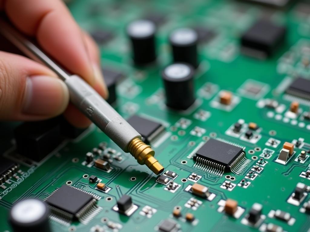
The Rise of Laser Depaneling: Precision Without Contact
레이저 디패널링 is the cutting-edge 디패널링 기술. It uses a 원자 램프 beam to cut through the 피씨비 재료 without physical contact. This process is exceptionally precise, generating a cut kerf width ~의 less than 20 microns, making it ideal for separating smaller and more complex boards, as well as flex pcbs 그리고 민감한 구성 요소.
What are the Advantages of Laser Cutting in PCB Separation?
레이저 커팅 isn’t just about fancy technology; it offers real benefits. One key advantage is the minimal 기계적 응력 it imposes, leading to better board integrity. The laser can also easily handle complex shapes and fine details, and it’s ideal for cutting individual circuits with very narrow gaps. It’s become a critical tool for modern pcb 생산, and the technology continues to evolve.
How Does Automation Benefit My Depaneling Process?
Automation is now key in any modern pcb 제조 process, and 디패널링 예외는 아닙니다. 자동화됨 디패널링 기계 not only increase 처리량 but also improve consistency and reduce human error. It is crucial to integrate automated 디패널링 시스템 당신의 생산라인 to maximize efficiency and keep up with the demand for PCBs는. We offer a variety of automation solutions tailored to meet your specific requirements.
Choosing the Right Depaneling Method: A Practical Guide
So, how do you pick the right 디패널링 method? It isn’t a one-size-fits-all decision. It’s about understanding the design of a panel, the type of materials, production volumes, the required accuracy, and the budget. We provide a practical consultation to guide you every step of the way, ensuring that your 디패널링 프로세스 is as efficient and effective as possible. We understand the subtleties of pcb 설계 and the critical needs of the 제조 공정.
My Experience and Expertise in PCB Depaneling Solutions
I’ve been in this business for over 20 years and have seen the production of printed circuit boards transform. I’ve also seen the rise of all types of pcbs and the increasing demand for smaller and more powerful 전자부품. My experience has taught me the importance of a well-optimized 디패널링 process. It’s not just about cutting the boards but also about maintaining quality and consistency, which are so crucial in pcb 조립. I’m sharing my knowledge with you, so you can avoid common pitfalls and optimize your 제조 공정.
Mechanical Routing Deep Dive
Let’s talk more about mechanical 라우팅. This method uses a specialized 라우터 bit to mill away the material that connects the PCBs는 within the pcb panel. The speed of the 라우팅 is dependent on the material of the 피씨비, the thickness of the material, and the complexity of the path. The accuracy is also greatly impacted by the quality and type of bit being used.
Pros:
- 비용 효율적: It’s a relatively affordable method, especially for larger, simple boards.
- 변하기 쉬운: It works on various types of pcbs.
- Established Technology: Widely understood and implemented.
Cons:
- Dust and Debris: It can create dust, requiring cleanup and potentially affecting 청결.
- 기계적 응력: The cutting action can induce some 기계적 응력, which can damage 민감한 구성 요소.
- 속도: Slower compared to some of the more advanced methods.
I’ve seen 라우팅 work wonders in high volume setups that have lots of boards of a similar shape and size. The 라우터 head is moved using computer controls and very little operator interaction is needed. This makes it very repeatable and reliable.
V-Groove Depaneling: Simplicity and Speed
V-그루브 depaneling stands out for its simplicity. A V-shaped groove or v-점수 is cut into the panel along the separation lines, and the 개별 pcb are then broken apart. This process is ideal for panels designed with straight lines of separation between the individual circuits.
Pros:
- 속도: It is a very fast separation process.
- Low Cost: It is an economical method for designs suited for it.
- Simple: It is an easy method to learn and implement.
Cons:
- Design Limitations: Only works with straight-line separations.
- Potential for Rough Edges: Can create rough edges which sometimes require additional cleanup.
- 기계적 응력: Breaking the panels can cause stress which can affect the integrity of the 땜납 and the connections.
I’ve witnessed V형 홈 depaneling excel in environments where there are individual printed circuit boards arranged in a grid format. The straight lines and high-speed separation process is a match for 고처리량 lines. However, when the designs get more complex, this solution is not a match.
PCB Punching: Speed at the Cost of Flexibility
펀칭 is another mechanical method that is used to cut the 개별 pcb from the larger panel. 펀칭 requires the creation of a die, which is created for each unique 피씨비 shape. This process is fast but the requirement for the die is very limiting.
Pros:
- High Speed: Very fast separation for large panels.
- 깨끗한 컷: When implemented correctly, the process can create very clean cuts.
- Repeatable: Very consistent across large runs.
Cons:
- Limited Designs: Not suitable for pcb 설계 with curves and fine features.
- Costly Tooling: Creating the custom 도구 그리고 고정물 is expensive and not good for small runs.
- 기계적 응력: The punching process can create a lot of 기계적 응력 to the components on the edge of the board.
I’ve seen this type of method used when the designs are relatively simple and the production numbers are very large. For instance, if there are just a handful of parts on the 피씨비, then the 펀치 process can make a lot of sense. It’s a good solution for simple shapes but it quickly becomes unsuitable if the shapes are more complex.
레이저 디패널링: 정밀의 미래
레이저 디패널링 is the most modern 분리 과정 and is accomplished by using a focused 원자 램프 beam. The 원자 램프 beam is used to remove the 피씨비 material. The non-contact nature of this process, makes it ideal for sensitive materials and complex shapes. The non-contact nature of the cut also reduces the amount of 기계적 응력.
Pros:
- 정도: It offers incredibly precise cuts, ideal for small or complex designs.
- 최소한의 스트레스: Non-contact cutting reduces 기계적 응력.
- 유연성: Can handle curves, sharp corners, and a wide range of materials.
Cons:
- 비용: High initial investment but lower recurring cost in some cases
- 속도: It can be slower when compared to some of the other processes but this can depend on a few factors.
- Setup: It can take some time to configure, especially when a lot of different shapes or types of pcbs are being created on the same line.
I’ve seen 레이저 디패널링 implemented in a lot of pcb 제조 environments that create flex pcbs and also smaller rigid pcbs. It’s truly one of the most exciting technologies in modern pcb 생산. It allows the creation of very complex designs and it is ideal for situations where 기계적 응력 is a concern.
Automation: Boosting Efficiency and Precision
The incorporation of automation in the 디패널링 프로세스 significantly boosts efficiency and reduces human error. Automation can take the form of an 인라인 디패널링 system that handles the 분리 과정 and passes the 개별 pcb directly into the next stage of the 생산라인. There are also systems that simply collect the boards for removal at a later time.
Pros:
- 처리량 증가: Automated systems can increase production line speed and reduce costs.
- 일관성: Provides highly consistent results, with every board being processed identically.
- 인적 오류 감소: Automated processes eliminate mistakes caused by operator error.
Cons:
- Initial Investment: Automated solutions can be an expensive up-front investment, although they pay off in the long term.
- Complexity: Can be complex to set up and integrate into an existing line.
- 유지: Requires regular maintenance and skilled staff to keep the equipment in top condition.
I’ve witnessed how systems that increase production line speed can be a game-changer in pcb 제조 plants. With the right automation, pcb 생산 can not only be faster, it can also be more cost-effective and reliable.
Making the Right Choice: Key Considerations
The best 디패널링 method is not one-size-fits-all, and the decision must be made on a case-by-case basis. Here are some of the key considerations you should make:
- PCB Design Complexity: Simple designs, with straight lines, can benefit from V형 홈 methods, while complex designs and flex pcbs require a 원자 램프.
- 생산량: 펀칭 or highly automated 인라인 디패널링 solutions can be ideal for large runs, but smaller runs may be more cost-effective with a 라우터 또는 원자 램프.
- 예산: Your budget will dictate the type of machine and the level of automation you can afford.
- Material Sensitivity: 레이저 디패널링 is the go-to solution when you have very 민감한 구성 요소.
- Throughput Needs: If high line speed and reduce costs is key, you need an automated system.
- Cleanliness: If the environment needs to be very clean, a 원자 램프 may be the right way to go.
It’s important to note that the need for systems that increase production line speed will continue to rise, and as such, the need for reliable 디패널링 해결책은 also continue to rise.
자주 묻는 질문
- What is the difference between depaneling and singulation? Both terms refer to the same 분리 과정 그만큼 individual printed circuit boards from a larger pcb panel. 디패널링 is most often used but 싱귤레이션 ~이다 also called it.
- How can I prevent 기계적 응력 during depaneling? Use non-contact methods such as 레이저 디패널링 or carefully designed mechanical setups with the right 고정물 to provide enough one part and supports for the 피씨비.
- What are the essential steps in choosing a 디패널링 시스템? Consider your pcb 설계, production volume, material sensitivity, required precision, and budget. A thorough assessment will help you choose the best method.
- 할 수 있다 레이저 디패널링 handle different types of pcbs? 예, 레이저 디패널링 is versatile and can be used on rigid pcbs, flex pcbs, and boards with very 민감한 구성 요소. It is excellent for all types of pcbs.
- How often should 디패널링 기계 be serviced? Regular maintenance is important and should be done according to the manufacturer’s guidelines. This will ensure the highest level of reliability and precision.
요약: 주요 요점
- 디패널링 중요한 단계입니다 pcb 제조, where 개별 pcb are separated from a 더 큰 패널.
- The best method depends on the design of the panel, material type, production volume, and budget.
- Mechanical 라우팅 is versatile and cost-effective, suitable for a wide variety of boards.
- V형 홈 is fast and efficient for panels with straight-line separations, but has 설계 limitations.
- 펀칭 is ideal for very large runs of simple designs, but has high 도구 costs and isn’t suitable for complex shapes.
- 레이저 디패널링 offers exceptional precision and minimal 기계적 응력 and is a good way to go when the boards are more complex or if 청결 is a concern.
- Automation can increase production line speed and reduce errors significantly.
- Careful selection of a 디패널링 method is essential to maintain quality and consistency.
- Always consider the need for systems that will increase production line speed to meet the demands.
Ready to take your pcb 제조 to the next level? 오늘 저희에게 연락하세요 for a consultation and let’s find the perfect 디패널링 solution for your needs. We pride ourselves on delivering top-tier depaneling machines that cater to the needs of giants in the electronics industry – and we’re here to bring that same expertise to you. Be sure to check out our PCB 라우터 기계, V-홈 디패널링, PCB/FPC 펀칭기, 자동장비, 부속품, 그리고 SMT 전체 라인 장비 solutions as well. Let’s work together to ensure your 생산라인 is both efficient and effective. With us, you’re not just buying machines, you’re investing in quality and expertise.