![]()

PCB depaneling for telecommunications
Revolutionizing PCB Depaneling: Exploring Laser, Router, and More for Automotive and Beyond
Hey there, fellow innovators and PCB enthusiasts! With over 20 years immersed in the intricate world of PCB manufacturing, I’ve witnessed firsthand the evolution of depaneling techniques. From the traditional methods to the cutting-edge laser technologies, I’ve seen it all. This article isn’t just another overview; it’s a journey through the most effective and efficient pcb 디패널링 방법, tailored to help you choose the perfect solution for your needs, especially in demanding sectors like the automotive industry. Whether you are involved in pcb 조립 for complex 전자 장치 or looking for a solution to 분리된 당신의 개별 인쇄 회로 기판, you’re in the right place. Let’s dive in and explore the fascinating world of 피씨비 singulation.
What is PCB Depaneling, and Why is it Crucial?
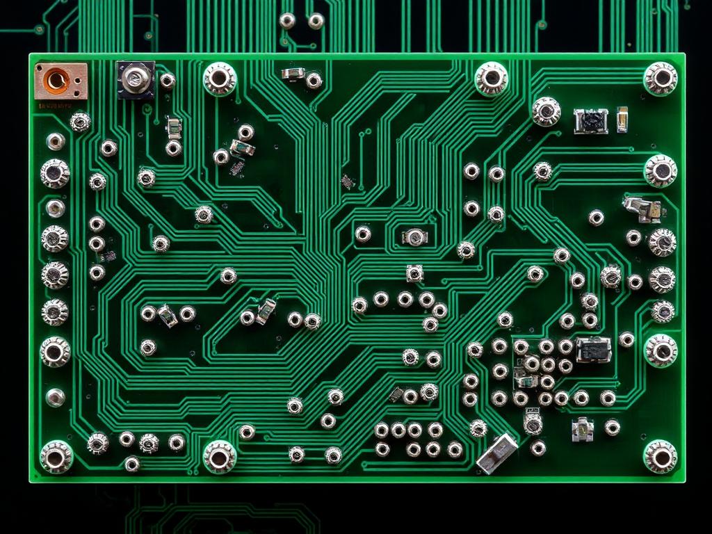
Let’s get started. PCBs are typically manufactured in 더 큰 패널 formats, containing multiple copies of the desired 회로 design, which is very crucial for pcb 제조. This approach streamlines the 제조 공정, allowing for faster and more cost-effective production. However, before these 인쇄 회로 기판 can be integrated into final products, the individual circuits must be 분리된 from the panel – that’s where pcb 디패널링 comes in.
PCB 디패널링, which is also called singulation, is the process of removing individual printed circuit boards from the larger panel. This crucial step is necessary in pcb 조립 as it transforms the panel into usable, individual boards ready for use in electronic products. The quality of the 디패널링 프로세스 significantly impacts the final product’s quality and reliability. It must ensure no 기계적 응력 or damage occurs to the 민감한 구성 요소 에 회로기판.
What are the Main Depaneling Methods for PCBs?
Over my two decades in the field, I’ve seen a variety of methods employed for separating PCBs는. Each method has its own advantages and disadvantages, making certain approaches more suitable for specific applications. Here are some of the most common 디패널링 방법:
- V-홈 디패널링: One of the most common pcb 디패널링 방법, this technique uses a v-점수 to create a weak line on the panel before the individual boards are 분리된. This is usually a one of the most common technique, however, it is not very precise and might be unsuitable for smaller PCBs는.
- 라우터: Using a 밀 또는 라우터, this method cuts out the individual 회로 기판 에서 패널 along a predetermined path. This method is highly versatile and provides a good balance of precision and speed.
- 펀칭: Employing a die, this method rapidly 분리된 개인 PCBs는, suitable for mass production with simple 절단선 designs. The use of punch is one of the most cost-effective techniques.
- 레이저 디패널링: This advanced method utilizes a 레이저 빔 to precisely 분리된 개인 PCBs는. It’s highly accurate, suitable for both 플렉스 PCB and rigid boards, and reduces 기계적 응력.
The choice of method often depends on factors such as material, desired 정도, panel complexity, and production volume.
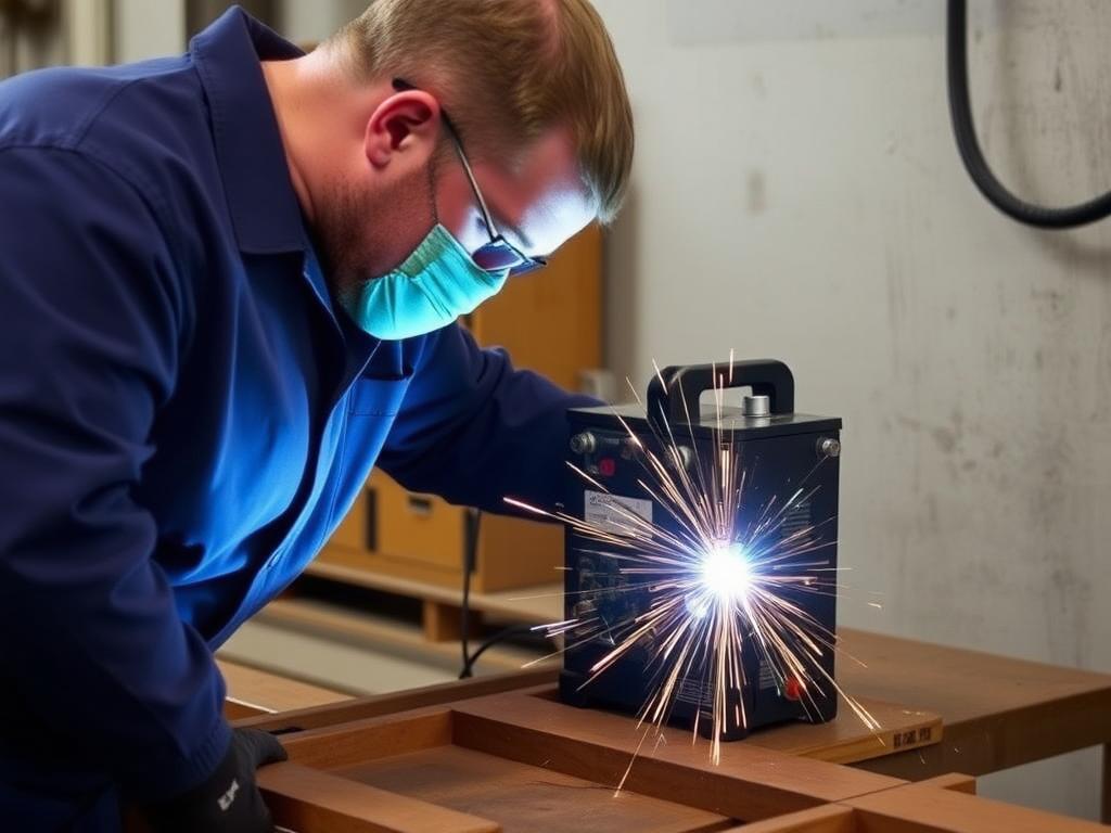
Why Choose Laser Depaneling for PCBs?
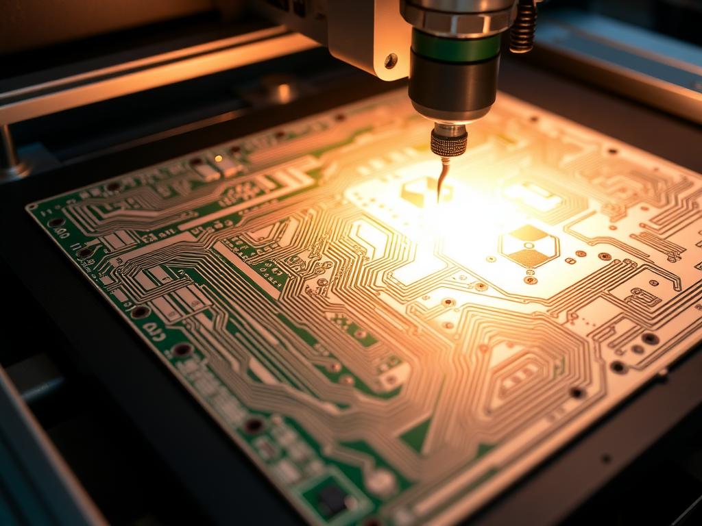
내 경험에 따르면, 레이저 디패널링 is a game-changer, particularly when precision and minimal stress are critical. Unlike methods that apply physical force, 레이저 pcb 디패널링 집중된 것을 사용합니다 레이저 빔 통과하다 기판 의 피씨비 without any physical contact. Here are a few reasons why 원자 램프 is rapidly becoming the preferred choice for pcb 절단:
- 높은 정밀도: 그만큼 원자 램프 비교할 수 없는 것을 제공합니다 정도 with a fine focused 레이저 빔, ensuring clean and accurate cuts with a very narrow 커프를 자르다, especially important for PCBs는 with delicate and 민감한 구성 요소.
- 감소된 기계적 스트레스: Because it’s a non-contact 절단 방법, 레이저 디패널링 minimizes the 기계적 응력 에 피씨비 동안 디패널링 프로세스. This is very important, especially for 몸을 풀다 PCBs는 and thin boards where even slight pressure can cause damage.
- 다재: From complex designs to various materials, a 원자 램프 can handle it all, including both rigid and 플렉스 PCB. This versatility allows for a wider range of applications, making it a go-to option for diverse pcb 제조 필요.
- Clean Cut Edges: This method provides very clean cut edges, reducing the risk of debris or burrs, which are crucial for ensuring technical cleanliness in applications.
How Does Laser Technology Benefit the Automotive Industry?
그만큼 automotive industry is at the forefront of technological advancements, and 레이저 기술 plays a pivotal role in this transformation. Given the stringent requirements for reliability and durability in automotive applications, using 원자 램프 ~을 위한 pcb 디패널링 offers significant advantages:
- High Reliability: 레이저 디패널링 보장합니다 PCBs는 used in vehicles are free from damage caused by physical pcb 디패널링 방법. This is very important in an environment where boards have to perform in harsh conditions, assuring the quality and reliability ~의 전자 장치 in automobiles.
- Complex Designs: 레이저 커팅 복잡한 것을 허용합니다 절단선 designs, essential for the miniaturization of electronic components in modern vehicles.
- Adaptable Process: This method is adaptable to the continuous innovation in 자동차 electronics, which allows for easy adjustments to process changes, and allows quick turnaround.
- Reduced Risk of Contamination: Maintaining a high standard of 청결 is a must in 전자 제조, and the non-contact method of 레이저 디패널링 minimizes the risk of contamination during the 디패널링 프로세스. This is especially important for sensor and control systems used in cars.
With the automotive industry continuing to embrace cutting-edge technology, 레이저 디패널링 is proving itself to be a very essential tool for producing high-quality, reliable electronic components.
Are There Other Viable PCB Cutting Methods Besides Laser?
하는 동안 레이저 디패널링 offers many benefits, other pcb 절단 methods remain relevant, especially when budgets or other constraints are a concern. The choice of method is highly dependent on specific requirements and priorities. Here are some alternative methods:
- V-Cut/V-Score: This 절단 방법 is cost-effective for straight line 분리된 and is commonly used in high-volume production for simpler 회로 designs. The main advantage is cost-effectiveness.
- 라우터: 아 라우터 with a mill is very flexible and provides good 정도 for complex 절단선 designs. However, this can create dust, and special equipment should be used to keep the area clean.
- 펀치: This approach is ideal for high-speed and high-volume 분리된 ~의 PCBs는 that have simple shapes.
The decision to go with a laser, 라우터, punch or another method will depend on multiple factors, including the cost, the specific requirements of your application and what you are looking for.
How Does a Router Compare to Laser in PCB Depaneling?
When comparing a 라우터 에게 원자 램프 ~을 위한 pcb 디패널링, it’s clear that each has its advantages. The key difference is in how the 제거 과정 그만큼 individual printed circuit boards is achieved.
에이 라우터 uses a milling tool to cut through the 피씨비 along a predetermined path, offering good 정도 and adaptability. It’s a cost-effective solution for various designs and materials and provides high 처리량. However, the physical contact with the 회로기판 during the milling process can produce dust, and can exert some degree of 기계적 응력 and can be noisy.
In contrast, 레이저 디패널링 is a non-contact method, using a 레이저 빔 to cut through the material. This approach offers very high 정도, minimal 기계적 응력, and very clean cut edges without debris. However, the initial investment in 레이저 시스템 can be higher compared to routers.
The table below summarizes a comparison between 라우터 그리고 원자 램프:
| 특징 | 라우터 | 원자 램프 |
|---|---|---|
| 정도 | 좋은 | 높은 |
| 기계적 응력 | 보통의 | 최소 |
| Material Versatility | 좋은 | 매우 높음 |
| 속도 | 좋은 | 높은 |
| Dust/Debris | 보통의 | 최소 |
| 초기 비용 | 낮추다 | 더 높은 |
| Complexity | Suitable for most | Suitable for everything |
Ultimately, the choice between a 라우터 그리고 원자 램프 depends on your specific requirements, budget, and desired results.
What Role Does Precision Play in PCB Depaneling?
정도 에 중요하다 pcb 디패널링, and one of the most important factors in ensuring the quality and reliability of electronic products. Inaccurate 디패널링 can lead to damage to the 피씨비 and its components, which can cause malfunctions or complete failure.
For very sensitive applications, like medical devices or automotive applications, 정도 is a must. The tighter the tolerances on 절단 속도, 그 커프를 자르다 width, and the position of the cut, the better the quality of the final product. 레이저 디패널링 가장 높은 것을 제공합니다 정도, achieving cut kerfs that are extremely narrow, which is crucial in reducing the amount of material wasted and enabling the production of smaller, more complex electronic circuits.
What are the Challenges of PCB Depaneling and How to Overcome Them?
Despite all the advancements, pcb 디패널링 comes with its fair share of challenges. Some of these challenges include:
- 기계적 응력: Methods like punch or V컷 can induce 기계적 응력, which can damage the components, especially for flex pcbs and thin boards.
- Dust and Debris: 라우터 그리고 밀 operations can produce dust, which, if not managed correctly, can cause contamination and affect the final product.
- Material Limitations: Not all 절단 방법 are suitable for all 피씨비 materials. For instance, some materials might not be suitable for V컷.
- 정확성: Achieving high 정도 with some of the older methods can be tricky, especially when working with complex designs.
To overcome these challenges, you have to utilize the right techniques and technologies. Using 레이저 시스템 그리고 고급 디패널링 시스템 can minimize 기계적 응력 and reduce the risk of contamination. Additionally, continuous monitoring and strict adherence to technical cleanliness protocols are essential.
How Can Advanced Depaneling Systems Improve Manufacturing Process?
고급의 디패널링 시스템 incorporate features that streamline the 디패널링 프로세스, reduce errors, and improve overall efficiency. Here are some ways these systems enhance the 제조 공정:
- 오토메이션: 고급의 디패널링 시스템 ~와 함께 오토메이션 reduce human error and speed up production, which leads to higher 처리량.
- 실시간 모니터링: Modern systems use sensors that monitor the 디패널링 프로세스 in real-time, helping to detect any potential problems as they occur.
- 유연성: Advanced systems are adaptable, allowing for quick switching between 피씨비 types and 절단선 designs, which is useful in dynamic production environments.
- Data Analysis: Many systems can gather data about the 프로세스, allowing users to quickly locate bottlenecks or problems, which will reduce costs.
- Integrated Cleaning: 일부 고급 디패널링 시스템 include cleaning stations, helping maintain high standards of 청결.
These advanced 디패널링 시스템 play a crucial role 현대에 전자 제조, and help increase efficiency, and ensure the production of high-quality PCBs는.
How Do I Choose the Right PCB Depaneling Solution for My Application?
올바른 것을 선택하기 pcb 디패널링 solution is a complex task that needs a comprehensive understanding of your specific needs. Here are some questions you should consider before making your choice:
- What type of 피씨비 are you working with? Are they rigid, flexible, or a combination?
- What level of 정도 is needed for your project?
- What is the volume of production?
- How sensitive are the components on the 회로기판?
- What’s your budget?
올바른 것을 선택하다 디패널링 시스템 needs a lot of careful planning and consultation with the experts. Understanding your needs and knowing the different types of 디패널링 방법 is the first step toward making an informed decision.
We are the world’s leading PCB depaneling machine manufacturer, with our products loved by TP-LINK, Canon, BYD, Flex, TCL, Xiaomi, Lenovo, OPPO, HONOR, Foxconn and other Fortune 500 customers. Our extensive experience and technical expertise can help you find the right solution for your specific needs. Whether you’re looking for 레이저 pcb 디패널링, 고속 라우터, or any other 디패널링 시스템, we are here to assist you. 문의하기 today to learn more about how we can optimize your pcb 조립 선.
자주 묻는 질문
주요 차이점은 무엇입니까? 레이저 디패널링 그리고 라우터 depaneling? 레이저 디패널링 is a non-contact method that uses a focused 레이저 빔 통과하다 피씨비, providing very high 정도 그리고 최소한 기계적 응력. 대조적으로, 라우터 depaneling uses a milling tool to physically cut through the 피씨비, which is often a good balance of speed and 정도, but can generate dust and impose some degree of stress.
~이다 레이저 디패널링 suitable for all types of PCBs는? 예, 레이저 디패널링 is very versatile and suitable for a wide range of PCBs는, including rigid boards, 플렉스 PCB, and more. It also works well on different materials, including 프르4.
할 수 있다 레이저 디패널링 handle complex and intricate designs? Absolutely! One of the key advantages of 레이저 디패널링 is its ability to cut complex and intricate shapes, making it very suitable for advanced electronic devices that have precise 절단선 디자인.
의 장점은 무엇입니까? V컷 depaneling, and what are its limitations? V-cut depaneling is very cost-effective, especially for high-volume production that involves a straight 절단선. However, it lacks the 정도 needed for complex designs and can result in 기계적 응력 ~에 민감한 구성 요소.
What is the role of technical cleanliness ~에 pcb 디패널링? Technical cleanliness is a very important aspect of pcb 디패널링, 특히 전자 장치 where contaminants can impact functionality. Methods like 레이저 디패널링 help ensure technical cleanliness by minimizing the generation of dust or debris.
주요 요점
- PCB 디패널링 는 중요한 단계입니다 pcb 조립 그리고 제조 공정, where 개별 인쇄 회로 기판 are separated.
- 레이저 디패널링 offers superior 정도, minimal 기계적 응력, and clean cuts, making it suitable for automotive applications and other high-precision sectors.
- 라우터, 펀치, 그리고 V컷 methods remain relevant for specific applications where cost or throughput are crucial factors.
- 고급의 디패널링 시스템 enhance efficiency through 오토메이션, real-time monitoring, and flexibility.
- 올바른 것을 선택하기 pcb 디패널링 solution requires a comprehensive understanding of your specific needs, budget, and application.
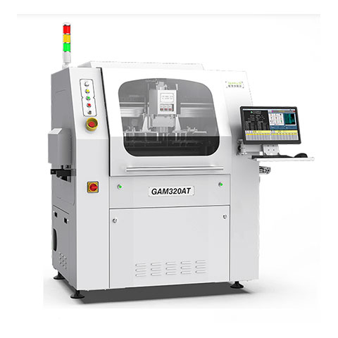
I hope this journey through the world of pcb 디패널링 has been insightful. If you’re ready to elevate your pcb 제조 capabilities, consider our range of advanced depaneling solutions. We are here to help you make informed decisions. You can learn more about our GAM 380AT PCB 바닥 디패널링 기계, explore options for V-홈 디패널링, or check out our PCB/FPC 펀칭기. Also make sure to take a look at our accessories to find the needed cutting heads. You might also be interested in our 자동장비. To explore your options for PCB 레이저 디패널링 or get expert advice, please do not hesitate to 문의하기 today! Let’s create a better, more efficient future together!