![]()

PCB depaneling for consumer goods
Precision PCB Depaneling: Choosing the Right Method for Your Circuit Boards
As someone with two decades immersed in the world of PCB manufacturing, I’ve witnessed firsthand the critical importance of pcb 디패널링. It’s the final, often overlooked, step that transforms a panel of connected circuit boards into individual, functional units. This article isn’t just about the technicalities; it’s about sharing my experience and guiding you toward the most effective depaneling solutions for your specific needs. Whether you are a large electronic product processing factory, an electronic technology company, or even an individual PCB enthusiast, understanding the nuances of depaneling is crucial. This detailed guide will cover everything from 레이저 디패널링 그리고 라우터 시스템 에게 V-홈 그리고 punching methods, all while keeping in mind the high-volume demands and precision required by industries like TP-LINK, Canon, and BYD—companies that have trusted my work in this space.
In-Depth Look at PCB Depaneling
1. What Exactly is PCB Depaneling and Why Is It Important?
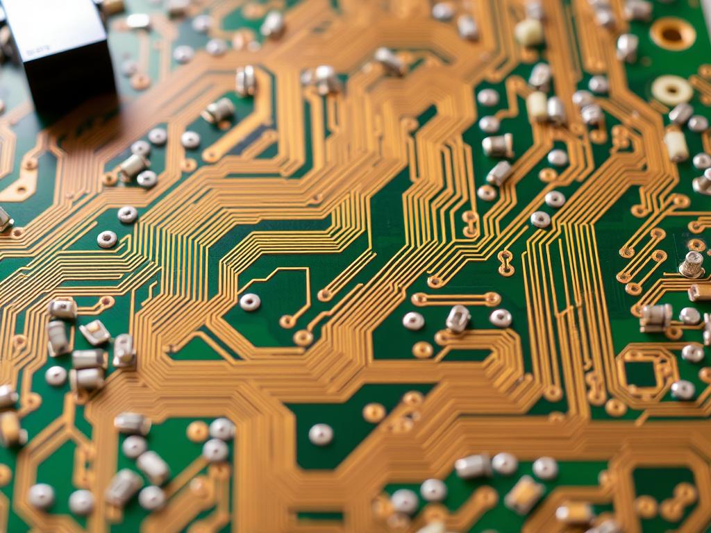
PCB 디패널링 개인을 분리하는 과정을 말한다 PCBs는 더 큰 패널에서 인쇄 회로 assembly process is complete. Imagine a sheet of postage stamps—that’s similar to how 인쇄 회로 기판 are manufactured on large panels to improve efficiency. The 디패널링 process is where these stamps become individual, ready-to-use circuit boards. This step is critical because it’s often one of the final stages of the manufacturing process, and any errors during 디패널링 can damage or render the finished 피씨비 unusable. Damage can also affect downstream processes like assembly into intended electronic devices, so the precision used is key. Over my two decades in the field, I’ve seen firsthand how crucial a smooth, precise 디패널링 프로세스 is to maintain high product yields and overall product quality. A good 디패널링 프로세스 must avoid 기계적 응력 that could lead to microscopic cracks in the 회로기판.
The importance of precise pcb 디패널링 cannot be overstated. Poorly executed 디패널링 can lead to various problems, including:
*   **Component Damage:** Mechanical stress can damage surface mount components, leading to functional failures.
*   **Microcracks:** Invisible cracks in the **pcb** substrate can occur, causing reliability issues over time.
*   **Edge Burrs:** Rough edges can make assembly more difficult and potentially cause short circuits.
*   **Reduced Product Lifespan:** Inconsistent **cut edge** quality can compromise the product's long-term durability.
*   **Increased Production Costs:**  Scrap and rework caused by bad **depaneling** significantly impact **production costs.**
효과적인 디패널링 ensures that the finished 회로기판 meets the high standards required for modern electronics.
2. What Are the Different PCB Depaneling Methods Available?
Over the years, I’ve worked with a myriad of 디패널링 방법, each with its own strengths and limitations. The right method often depends on the specific design, material, and production volume of your PCBs는. Here’s an overview of the most common 디패널링 방법:
*   **Laser Depaneling:** Using a **laser beam** to cut through the **pcb**, this method is ideal for complex shapes and delicate **pcbs**, and it has become more and more popular for its precision and versatility.
*   **Router Depaneling:** A **router machine** uses a high-speed milling bit to separate the **pcbs**. It’s a reliable choice for thicker or more robust **pcbs**.
*   **V-Groove Depaneling:** This method utilizes a special **v-groove** tool to score the **pcb** along predefined lines, making it easier to snap them apart. It’s ideal for simpler, rectangular **pcbs**.
*   **Punching Machine:** Uses a die to **punch** out individual **pcbs** from a panel. This is a high-throughput method suitable for mass production of simple shapes, especially **single pcbs are punched** out from larger panels.
*   **Die Cutting:** Similar to **punching**, but often used for more complex shapes, sometimes with flexible **pcb** material, and is also **used for cutting** out **pcb**.
Each of these methods has its place in the industry. However, advancements in technology, especially 레이저 기술, have greatly impacted the choices we make today. The goal is to choose a method that ensures the integrity of the board while optimizing 처리량 and minimizing production costs.
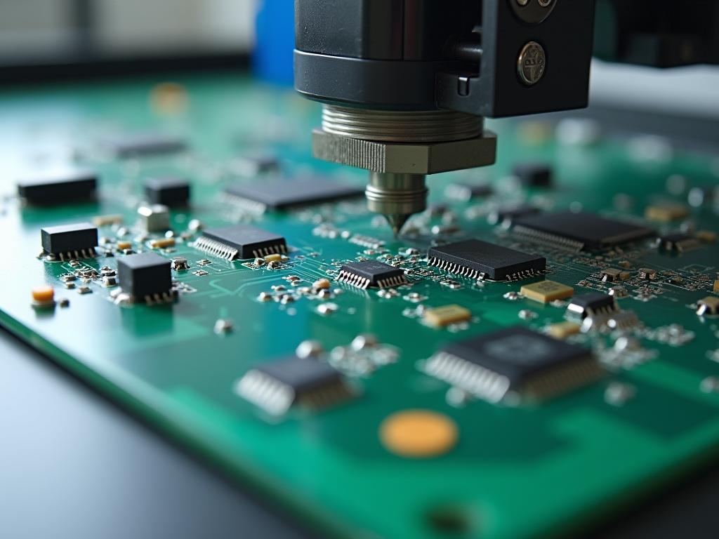
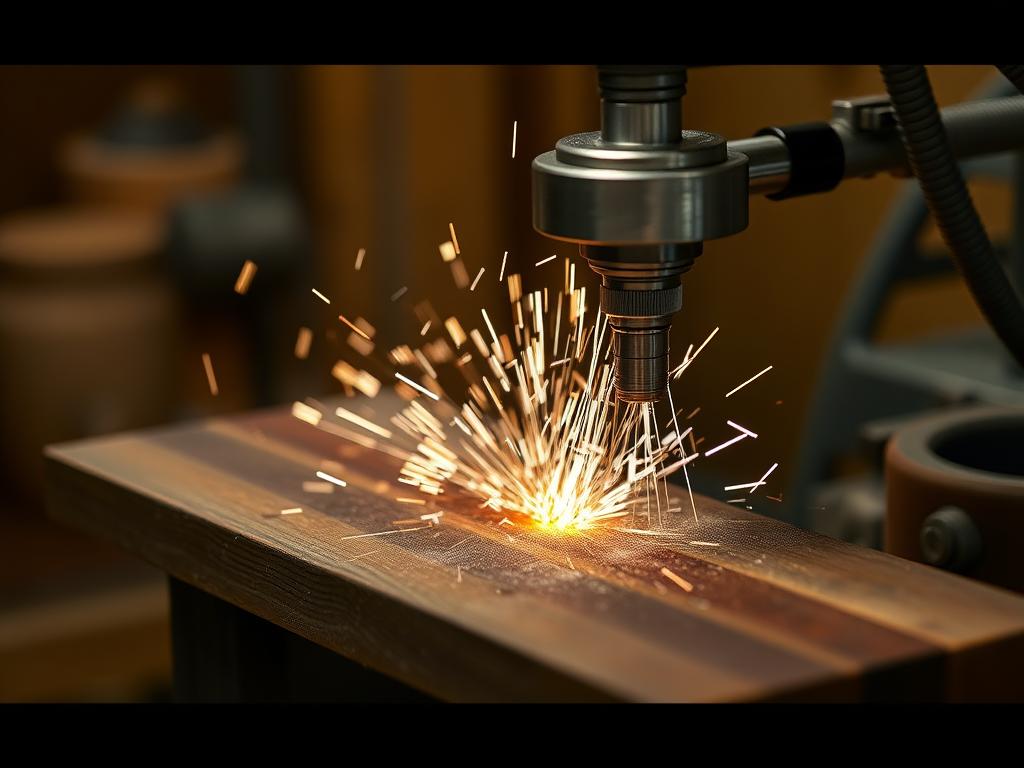
3. Why is Laser Depaneling Becoming the Preferred Method for Many?
레이저 디패널링 has revolutionized the way we handle 피씨비 separation, and over the past 5 to 10 years in particular I’ve noticed a tremendous shift toward this technology. It’s a sophisticated, non-contact method that offers unparalleled precision. Instead of a blade or physical force, 레이저 디패널링 집중된 것을 사용합니다 레이저 빔 to melt or vaporize the material along the cut edge, creating a clean, smooth separation. Key advantages include:
*   **Precision and Flexibility:** The **laser** can cut complex shapes with incredible accuracy. The **laser** can cut along arbitrary lines, enabling the **freeing pcb designers** from the limitations of other methods, especially for **multilayer pcb** designs.
*   **Minimal Mechanical Stress:** Because it’s a non-contact process, **laser depaneling** minimizes **mechanical stress** on the **pcb**, reducing the risk of component damage and microcracks which could be caused by **traditional mechanical cutting**
*   **Clean Cut Edges:** **Laser cutting** produces incredibly clean and precise **cut edge** results without burrs or dust, reducing the need for post-processing.
*   **Suitable for Delicate and Flexible PCBs:** Ideal for thin, flexible, and fragile **pcbs** where other methods might cause damage.
*   **Fast and Efficient**: **Cutting speed** is greatly increased.
Specifically, 자외선 레이저 technology has emerged as a game-changer. It delivers even finer control and precision, making it suitable for high-density interconnect PCBs는 그리고 재료 조합. 그 레이저 절제 공정 를 사용합니다 원자 램프 to vaporize the material, resulting in a very small 커프를 자르다. 의 진화 원자 램프 technology with the frequency-tripled laser emerged made 레이저 디패널링 a superior process. With high-precision, high-speed, and narrow 커프를 자르다, 그 레이저 공정 has become a workhorse. Our 레이저 디패널링 machines are designed for high-precision and high-speed manufacturing, enabling you to increase production while maintaining superior quality.
4. When is Router Depaneling the Best Choice for PCB Separation?
하는 동안 레이저 디패널링 offers many advantages, 라우터 depaneling remains a reliable and 비용 효율적 method, especially for certain types of PCBs는. I’ve used 라우터 머신 for years, and they remain a staple in many manufacturing environments. Here’s when router depaneling is a good fit:
*   **Thicker PCBs:** Routers are great for thicker **pcbs** or those with more robust construction where the **laser** may struggle with the **dielectric** layers.
*   **Straight Cuts and Basic Shapes:** If your **pcb** designs feature mainly straight lines or simple curves, **router** depaneling can handle these efficiently.
*   **Large Volume Production:** The speed and reliability of a **router** make it a solid choice for large-volume production runs, where high **throughput** is paramount.
*   **Cost-Effectiveness:** If you’re on a tighter budget, a **router machine** may offer a **more cost-effective** solution compared to the initial investment in **laser** equipment.
라우터 머신 use a rotating bit to cut the 피씨비 along pre-programmed paths. Although there is some mechanical stress and the cut edge may not be quite as smooth as 레이저 커팅, modern 라우터 머신 are designed to 최소화하다 vibration and achieve good results for many applications. When working with 라우터 머신 , the feed rates and spindle speeds play a crucial role in the quality of cut edge, therefore having the correct parameters is crucial for best results.
5. What Role Does V-Groove Depaneling Play in PCB Manufacturing?
V형 홈 디패널링 is a classic method that relies on pre-scored pcb, which is typically used to cut multiple boards in a panel. This technique is ideal when individual PCBs는 are rectangular or very close to rectangular, it’s all about making 손이 부러지다 efficient. A V-홈 machine uses a blade to score a V자형 channel into the 피씨비 along pcb를 따라 the separation lines which makes pcb depaneling refers to simply snapping the boards apart. Here’s a closer look:
*   **Simplicity:** It’s one of the simplest and most straightforward **depaneling methods**.
*   **Cost-Effective for High Volumes:** It is **cost effective** for high volumes for simple designs.
*   **Fast Separation:** The scoring process is quick, and the actual separation by snapping apart is very fast.
*   **Suitable for Specific Designs:** Best suited for rectangular **pcbs** with straight lines and minimal curves and is commonly used for **single boards are connected using tabs.**
Although V-그루브 디패널링 is cost-effective and fast, the trade-off is that it’s not suited for all PCBs는. 그 기계적 응력 from the breaking process can be problematic, especially for sensitive components. Also, this 절단 방법 does not offer much in the way of flexibility, but is great for large quantities of simple PCBs는 where the boards are connected using tabs. V형 홈 is a good option for high volume, basic, rectangular PCBs는 with minimal components in the scoring area.
6. What are the Advantages of Using a PCB/FPC Punching Machine?
PCB/FPC 펀칭 머신 are essential for high-volume production, particularly when simple shapes and fast cycle times are required. I’ve seen 펀치 machines in action in many large-scale facilities and when optimized they can deliver massive 처리량. This method uses a hardened die to physically 펀치 out individual PCBs는 or flexible circuits (FPC) from the larger panel. The advantages include:
*   **High Speed:** **Punch** machines offer the fastest **cutting speed** of the **depaneling methods** making them ideal for very high-volume production runs.
*   **Cost-Effective in Mass Production:** Once set up, the recurring costs for this **depaneling method** are minimal.
*   **Suitable for Simple Shapes:** Perfect for **pcbs** with basic shapes, such as squares, rectangles, and circles, where the die can be crafted without the need for complex tooling.
However, 펀칭 is not suitable for all PCBs는. It’s not flexible and is not suited for more complex shapes, nor is it ideal for delicate PCBs는 where mechanical stress needs to be minimized. The initial investment in the custom die can also be considerable, but the time and labor savings over the course of a massive production run far offset those cost challenges presented. 우리의 펀칭 머신 are robust and reliable, designed to keep up with your high production demands. 펀칭 is often utilized to produce individual boards need ~을 위한 home automation equipment.
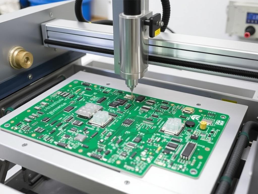
7. How Does Automation Enhance the PCB Depaneling Process?
오토메이션 is transforming every aspect of modern manufacturing, including pcb 디패널링. I’ve personally witnessed the huge impact that 오토메이션 can have on efficiency and consistency in a production environment, which is why automation solutions are key. Integrating 오토메이션 ~ 안으로 디패널링 yields several key benefits:
*   **Increased Throughput:** Automated machines can operate continuously, reducing human errors and significantly increasing **throughput**.
*   **Consistent Quality:** **Automation** ensures consistent cutting results, reducing defects and improving overall quality.
*   **Reduced Labor Costs:** By automating the **depaneling** process, you can minimize the need for manual labor, therefore reducing costs in **manufacturing process**.
*   **Improved Efficiency:** **Automation solutions** help optimize the entire production line, resulting in shorter lead times and greater productivity.
*   **Precise Handling**: Automated loading, unloading, and sorting systems ensure the **pcbs** are handled with care, minimizing any damages.
*   **Minimizing Human Error:** Automated systems are less prone to human errors.
우리의 자동 장비 such as the GAM 630V Automatic Sorting and Palletizing Machine and GAM 620H Automatic Tray Collecting Machine are designed to work seamlessly with our 디패널링 기계, creating a fully automated production system. This helps ensure the individual boards need for each product are quickly and accurately 패널이 분리됨. In our experience, 오토메이션 is essential for any high-volume manufacturing facility that wants to maintain consistent quality and maximize productivity.
8. What Are Some Essential Accessories for PCB Depaneling Machines?
The right accessories can dramatically improve the performance and lifespan of your 디패널링 기계. Over my time in the industry, I’ve learned the importance of having the right tools for the job. Here are some essential accessories:
* **Milling Cutters**: High-quality **milling cutters** are crucial for **router machines**, ensuring clean cuts and a long tool life.
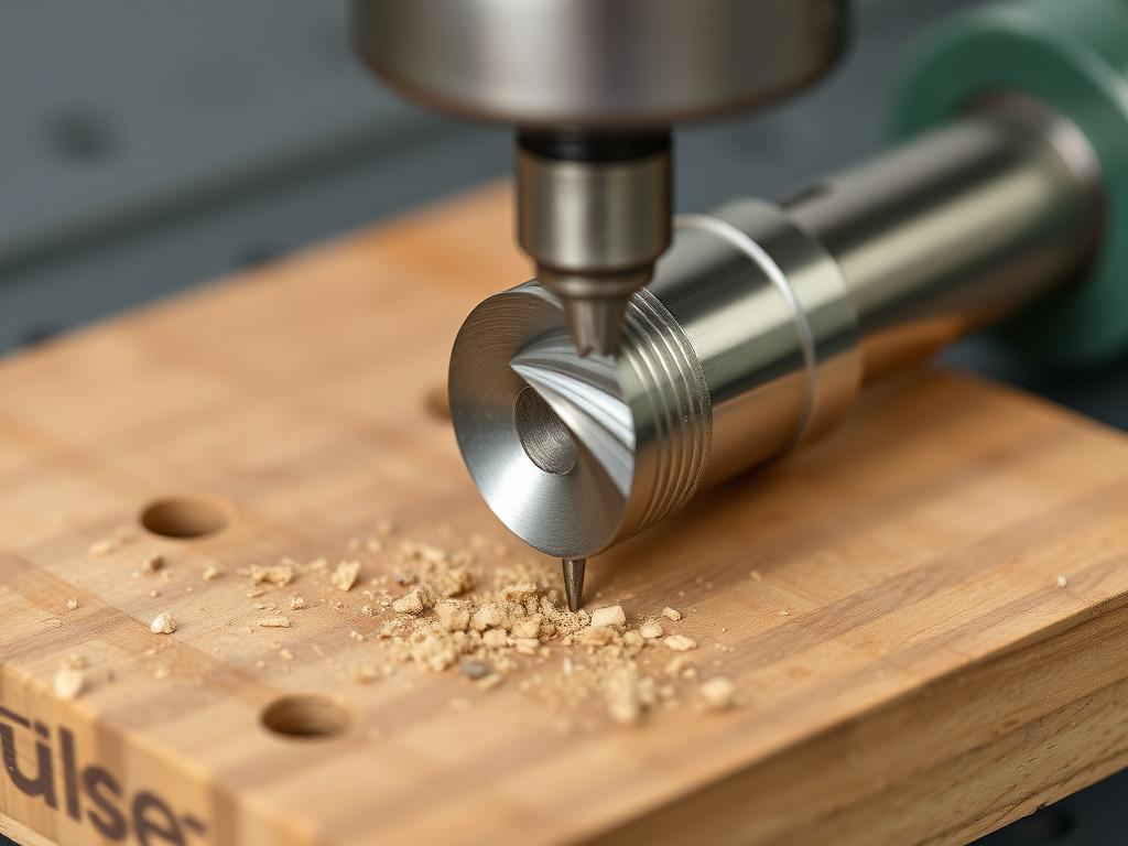
* **Laser Optics**: Precision lenses and mirrors are essential to maintain a focused and efficient **laser beam** and a **narrow kerf width**, ensuring precision and accuracy in **laser ablation process**.
* **V-Groove Blades:** For **v-groove depaneling**, the blade must be made from durable materials, and be precisely calibrated to ensure accurate scoring.
* **Punch Dies:** **Punch dies** must be precisely machined from hardened materials to ensure they produce a clean **cut edge** while maintaining longevity.
* **Dust Collectors**: Effective dust collection systems are essential for removing debris during **cutting is performed**, preventing contamination and machine damage.
* **Spindles**: High-precision spindles are vital for **router machines** to ensure smooth, vibration-free operation.
Investing in high-quality accessories may come at an initial cost, but it is worth it as it contributes to the overall efficiency, reliability, and precision of your 디패널링 프로세스. Quality accessories are an important part of a reliable manufacturing system, and they contribute significantly to the long term cost effectiveness of your operation. Our selection of accessories is designed to complement our 디패널링 기계, ensuring optimal performance and durability.
9. How Do Different SMT Lines Benefit from Efficient PCB Depaneling?
효율적인 pcb 디패널링 is critical for optimizing the flow of material through an SMT (Surface Mount Technology) production line. Over the last two decades, I’ve seen many facilities struggle with bottlenecks caused by inefficient or poorly planned 디패널링 processes. Effective 디패널링 is an integral part of a smooth SMT line. Here’s how efficient 디패널링 benefits an SMT line:
*   **Smooth Production Flow**: A good **depaneling system** ensures a smooth transition between the board assembly and the subsequent stages.
*   **Reduced Bottlenecks:** An efficient **depaneling process** prevents bottlenecks and keeps the entire line running smoothly.
*   **Minimized Damage**: Precise **depaneling** methods minimize damage, ensuring that the **pcbs** reach the next stage of the SMT line in perfect condition, and are ready for **downstream processes like** installation into their **intended electronic devices**.
*   **Increased Productivity**: By eliminating errors and ensuring a reliable **depaneling process**, an SMT line can achieve higher productivity and lower operating costs.
*   **Seamless Integration**: Properly designed **depaneling machines** can be integrated seamlessly with the automated material handling systems within an SMT line.
*   **Improved Quality:** Efficient **depaneling** ensures consistent quality throughout the entire manufacturing cycle.
Integrating a high-performance 디패널링 머신 into your SMT line is key to optimizing efficiency and quality, and it can become a real game changer for your production. Our SMT 전체 라인 장비, including our SMT 인라인 디패널링 머신 솔루션 그리고 라우터 머신 & 로봇 암 & 자동 플레이트 세팅 머신 are designed to integrate seamlessly with existing SMT lines, to optimize your workflow.
10. How to Select the Right Depaneling Method for Your specific application?
Choosing the correct 디패널링 방법 is crucial for ensuring the quality, efficiency, and profitability of your production. I’ve guided countless clients through this decision, and here’s my advice:
*   **Assess your PCB Design:** Consider the complexity, shape, and materials of your **pcbs**. Complex shapes and delicate materials favor **laser depaneling**, while simpler shapes may be suitable for **v-groove** or **punching**.
*   **Evaluate Production Volume**: High-volume production often benefits from **punching** or **router** methods, while low-to-medium volumes may be more suited to **laser depaneling**.
*   **Consider Cost**: Evaluate the initial cost of the **machine** and the ongoing operating costs, including maintenance and consumables.
*   **Quality Requirements**: High-precision applications may require **laser depaneling** for its clean **cut edge** and minimal mechanical stress.
*   **Flexibility**: If you need to handle multiple **pcb** designs, **laser depaneling** may offer the greatest flexibility for the cost.
*   **Space Considerations:** Assess the footprint of the **machine** and ensure it fits within your production area.
Choosing the correct method and 디패널링 시스템 is very complex and requires a thorough understanding of your requirements, and it can be challenging to get the best result. When you take all of these factors into account you can ensure that the selected 디패널링 방법 is aligned with your unique needs, and your long-term goals. By carefully considering these factors you can make an informed decision and choose a reliable and 비용 효율적 solution. Our team is here to provide expert advice and help you choose the 디패널링 방법 that best fits your requirements.
PCB 디패널링에 대한 FAQ
What is the difference between laser depaneling and router depaneling? Laser depaneling uses a laser beam to cut through the circuit board, offering precision and minimal mechanical stress. Router depaneling uses a high-speed milling bit, which is suitable for thicker boards.
레이저 디패널링은 모든 유형의 PCB에 적합합니까? Laser depaneling is versatile and suitable for a wide variety of PCB materials and designs, however, certain materials may not be suitable for a laser process.
Can I automate my PCB depaneling process? Yes, automated depaneling systems are available that can significantly increase throughput and reduce labor costs, and these can be integrated into your existing SMT line.
What kind of maintenance is required for a PCB depaneling machine? Regular maintenance, including cleaning, lubrication, and blade/cutter replacement, is necessary to keep the machine functioning correctly and reliably.
How much does a laser depaneling machine cost? The cost can vary depending on the capabilities and features of the machine. We offer a range of laser depaneling machines to fit various needs and budgets, please contact us for more details.
In Summary
- PCB 디패널링 is critical for separating individual PCBs는 더 큰 패널에서.
- Various methods are available, including 원자 램프, 라우터, V-홈, 그리고 펀치 depaneling, each suitable for different applications.
- 레이저 디패널링 offers high precision and minimal mechanical stress, making it ideal for delicate PCBs는 and complex shapes.
- Router depaneling is a reliable choice for thicker PCBs는 and straight cuts.
- V형 홈 디패널링 is best for simpler, rectangular PCBs는.
- Punch machines are suited to high-volume production of simple shapes.
- 오토메이션 greatly enhances efficiency and consistency in the 디패널링 프로세스.
- Proper accessories are crucial for maintaining the performance of your 디패널링 기계.
- 효율적인 디패널링 is essential for a smooth and productive SMT line.
- 올바른 것을 선택하기 디패널링 방법 depends on 피씨비 design, production volume, and budget.
I hope this comprehensive guide has been valuable. As you navigate your pcb 디패널링 needs, know that I and my team are here to provide you with the best solutions. We understand the challenges faced by electronic technology companies, large factories, and individual 피씨비 enthusiasts and we are committed to delivering the best performance and value.
Let’s discuss your depaneling requirements today. 문의하기 to see how we can help you optimize your production line.
Learn more about our: