![]()

International PCB depaneling technology
Precision PCB Depaneling: Choosing the Right Method for Your Needs
For over 20 years, I’ve been deeply involved in the fascinating world of PCB (printed circuit board) manufacturing. Depaneling, the process of separating individual circuit boards from a larger panel, is a critical step often overlooked, yet it significantly impacts the final product’s quality and reliability. This article dives into the various depaneling methods, focusing on laser depaneling technology and how it stacks up against other techniques. Whether you’re a large electronics processing factory, an electronic technology company, or an individual PCB player, understanding these options is essential for achieving optimal results. It’s worth reading because we’ll explore how to ensure optimal stress-free separation for your high-performance PCB designs.
PCB 디패널링이란 무엇이고 왜 중요한가?
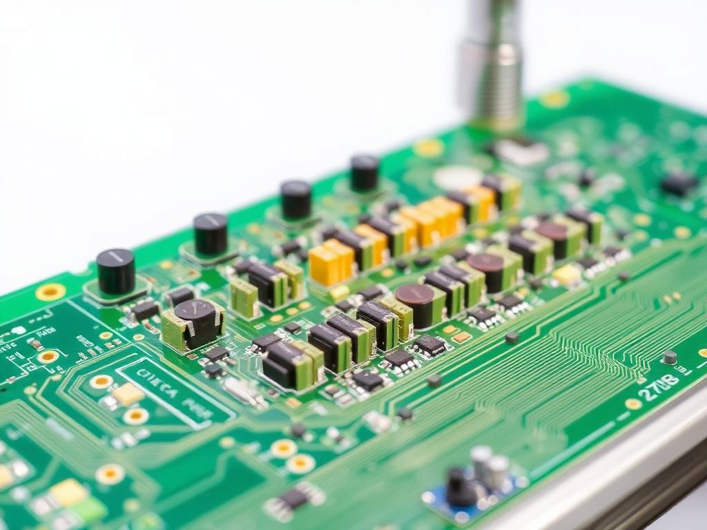
PCB depaneling, at its core, is the process of separating individual PCBs는 더 큰 패널에서 pcb 조립 process. Imagine a sheet of cookies, and you have to break them apart without damaging them. That’s essentially what depaneling is all about. Why is this so important? Because the method you choose directly affects the amount of 기계적 응력 applied to your 인쇄 회로 기판 during separation. Too much stress can damage sensitive electronic components, lead to micro-cracks, and ultimately, cause failures in the field. For years, I’ve seen first-hand how improperly separated pcb 보드 can compromise the entire process ~의 전자 조립. That’s why a well-chosen 디패널링 프로세스 is critical to the success of your product.
The goal is to achieve clean, precise separation while minimizing any stress to the pcb소재 itself. This becomes even more crucial with today’s trend toward smaller, more densely packed boards using surface mount SMT technology. Whether it’s a simple single-layer 인쇄 회로 or a complex multi-layer HDI (High Density Interconnect) board, the depaneling method has a huge impact on the final quality. Therefore, understanding the methods of pcb depaneling is paramount in ensuring high quality and reliability of products.
What are the Different Depaneling Methods?
Over the years, I’ve worked with numerous 디패널링 방법, each with its own set of pros and cons. Let’s look at some of the most common techniques:
- Hand Breaking: This is the most basic method, where boards are manually separated along pre-scored lines (often called v-스코어링). While it’s cost-effective for very low-volume production, it’s prone to uneven breaks and high 기계적 응력, potentially leading to component damage. It is definitely not the preferred method.
- V-홈 디패널링: Using a blade or a series of blades to cut through pre-scored V형 홈 is a step up from manual breaking. While more controlled, it still imparts stress to the board. This is used in low to medium volume.
- Punch Depaneling: A punch tool is used to separate the boards, ideal for simpler shapes. However, the impact can cause bending of the board, again leading to stress.
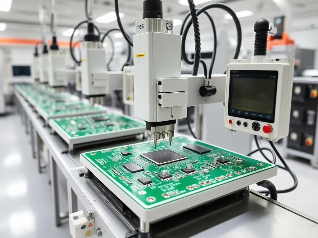
- Router Depaneling: This method employs a milling machine (밀) or 라우터 to cut around the boards. This allows for complex shapes and is less stressful than mechanical methods.
- 레이저 디패널링: This modern technique uses a 레이저 빔 to cut through the panel. It offers the highest level of 정도, generates the least amount of stress and is incredibly versatile.
The key thing to remember is that the best 디패널링 방법 for you depends heavily on your specific requirements, considering the pcb 설계, 그 사용된 재료, board thickness and the volume of pcb 생산.
레이저 디패널링은 무엇이고 어떻게 작동하나요?
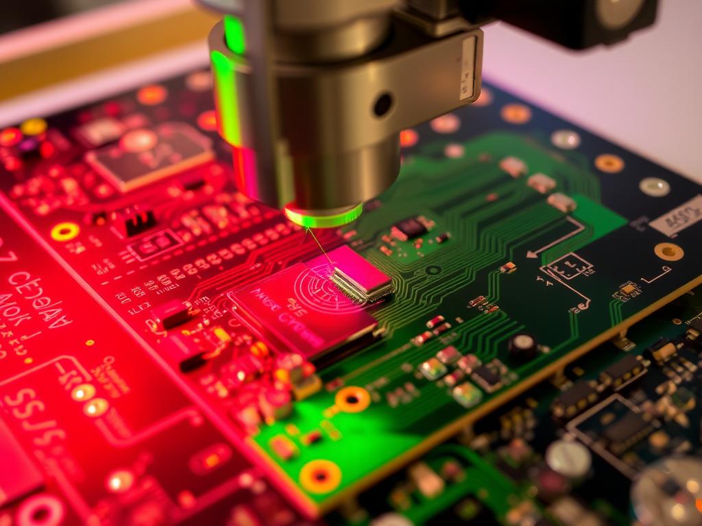
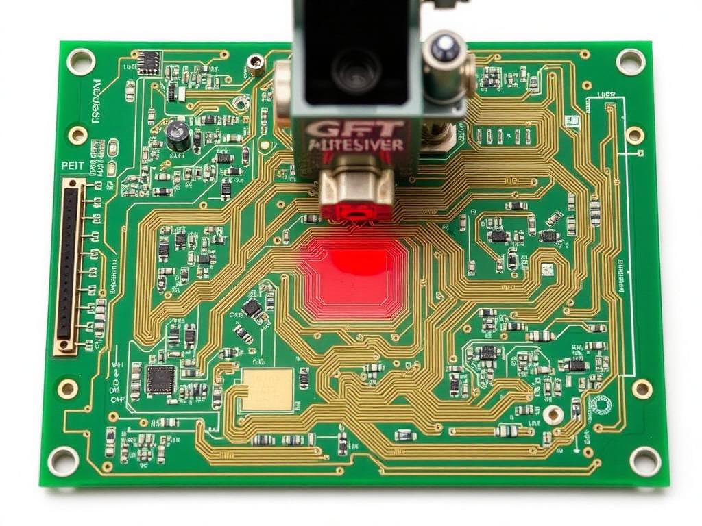
As a veteran in this industry, I’ve witnessed firsthand how 레이저 디패널링 has revolutionized the separation process. It is a non-contact process, meaning that the 원자 램프 is not actually touching the workpiece. It uses a focused 레이저 빔 to ablate or vaporize the pcb소재 along a predetermined path. The heat generated by the 원자 램프 is minimal and highly localized, which means that the rest of the 피씨비 is not affected by the heat.
The precision is the crucial factor here. Because the 레이저 빔 is so fine, we can achieve incredibly intricate cuts with exceptional accuracy. Moreover, this method imparts very little 기계적 응력 에게 PCBs는, making it ideal for sensitive electronic components. Whether it’s a thin 유연한 회로 or a rigid multi-layer board, 레이저 디패널링 provides consistent and high-quality results. The 레이저 공정 is controlled by software, which gives it consistent results compared to mechanical methods that suffer from wear and tear of tooling.
PCB에 레이저 디패널링을 선택해야 하는 이유는 무엇입니까?
Over my career, I’ve seen many companies struggle with traditional depaneling methods, which can lead to a lot of rework and wasted time. This is why when it comes to separating PCBs는, 레이저 디패널링 is often the preferred method. Here are the key reasons why:
- 최소 기계적 스트레스: Unlike mechanical methods that exert force on the pcb소재, 그 레이저 커팅 process is essentially stress-free. This is critically important for high-density boards with delicate components. For sensitive 전자부품, 레이저 디패널링 is the best solution as it does not damage the surface mount or through hole devices.
- 높은 정밀도: The focused 레이저 빔 allows for very fine cuts and complex shapes with high accuracy. This makes it suitable for even the most demanding pcb 설계.
- 다재: Lasers can cut through a wide range of materials, including FR4, flex circuits, and even metal-core pcb 보드. It can handle different board thickness ranging from 0.4 to 3.2mm or even more with custom made machines.
- 청결: 그만큼 레이저 커팅 process produces minimal dust, which is important in maintaining a clean production environment.
- 유연성: The cutting path can be easily modified via software, allowing for quick changes and handling of different pcb 설계 variants.
In short, if you value 정도, low 기계적 응력, and flexibility, 레이저 디패널링 is a game changer. It is very important that the equipment must work reliably with demanding requirements for a consistent outcome.
What Are the Benefits of Using Laser Technology in Depaneling?
Stepping into the more technical aspects of laser technology in depaneling, we can discover the key advantages that set it apart. A major benefit of 레이저 디패널링 lies in the type of 원자 램프 used. Typically, UV 레이저 systems are employed in PCB depaneling. UV 레이저 light is readily absorbed by a vast range of 기판 materials, resulting in clean cutting with minimal thermal stress.
Additionally, the 레이저 공정 offers superior edge quality compared to mechanical methods, where the edge of the cut can be rough. This reduces the risk of interconnect issues in the next assembly step. It is ideal for those who need the highest processing standards, 특히 high-performance applications. Also, 레이저 디패널링 systems can be easily integrated into automated production lines, further enhancing 처리량.
The high 정도 also reduces the need for a fixturing, the board can be processed as a part of the full panel or it can be processed as a single PCB within a 독립형 system. The system is very precise in the order to cut the individual single pcbs which makes the entire process flexible.
When Is 라우터 Depaneling the Right Choice?
하는 동안 레이저 디패널링 has many advantages, 라우터 depaneling still has its place in the manufacturing process. In my experience, routers are a great choice when you need to handle a very wide variety of board thickness with different shapes and sizes. They also allow a wider tolerance on the milling path without affecting the final result.
Here are some situations where 라우터 depaneling is a good option:
- Larger Board Thicknesses: For very thick boards, routers can handle them well, especially if the 사용된 재료 is very hard or brittle.
- Complex Shapes: While lasers can cut complex shapes, routers are more cost-effective when you have shapes that require deep channels or rounded corners.
- 비용 효율성: For large-volume production, 라우터 depaneling can be more 비용 효율적 when the high setup cost for 레이저 디패널링 is hard to justify.
- Larger Boards: It is common to see routers being used when dealing with PCBs는 that are large in size or not suitable for other separation methods.
Remember, 라우터 depaneling involves a mechanical tool, so there’s always some level of stress and dust generated during the 라우팅 프로세스.
What About V-그루브 그리고 펀치 Depaneling Methods?
From my 20-year experience, V형 홈 그리고 펀치 depaneling methods are considered more traditional ways to separate PCBs는. Let’s review when they might still be considered:
V-홈 디패널링: This method is characterized by making a “V” shaped cut on both sides of a panel and then snapping the board along that cut. This method is suitable for boards that are designed for this specific separation. Here is a typical case where I would consider it:
- Low-Cost Option: V형 홈 is an easy and 비용 효율적 option for simpler designs and mass production where extremely high precision is not required.
- Simple Designs: This method works best with straight lines and uniform shapes.
- Fast Throughput: This method has a high 처리량 as the machine is quick and does not require a lot of setup time.
Punch Depaneling: This method involves using a punch and die to separate individual PCBs는 from a panel. Here’s a situation in which I would consider using it:
- Specific Shapes: It is good for separating pre-defined shapes with a high level of consistency.
- High Volume: This method shines when separating large volumes of simple board shapes quickly.
However, both methods cause significant 기계적 응력, and the choice of cutting methods can lead to issues with sensitive components.
How Can 오토메이션 Improve Your Depaneling Process?
Throughout my career, I’ve seen that integrating 오토메이션 into the 디패널링 프로세스 can significantly improve efficiency, reduce errors, and lower costs. Automation allows for consistent and repeatable results, improving the overall quality of pcb 생산. The benefits of using 자동화 솔루션 다수 있습니다:
- 처리량 증가: Automated machines can process PCBs는 much faster than manual methods, significantly increasing 처리량.
- 노동비 절감: By automating the 디패널링 프로세스, you reduce the need for manual labor, resulting in significant cost savings.
- 향상된 품질: Automated systems offer higher 정도 and reduce the risk of human error, leading to higher quality PCBs는.
- Consistent Results: 오토메이션 ensures consistent and repeatable results, which is essential for maintaining high quality standards.
- 감소된 폐기물: By minimizing errors, 오토메이션 reduces the amount of scrap and rework, leading to less waste.
- Inline Integration: 자동화됨 디패널링 시스템 can be easily integrated 인라인 with other SMT equipment to provide a seamless manufacturing process. Whether you are using 원자 램프 또는 라우터 디패널링 기술, the addition of 오토메이션 can enhance productivity and reduce costs. From my experience, combining 오토메이션 ~와 함께 레이저 디패널링 is the most efficient way to separate PCBs는 especially in 고용량 생산.
How To Choose The Best 디패널링 머신 For Your Needs?
올바른 것을 선택하다 디패널링 기계 is essential for achieving high-quality results and optimal efficiency. There is no “one size fits all” solution. The ideal machine must be aligned with your specific requirements and business needs.
Here’s how you should approach this important decision:
- Understand Your Requirements: Start by evaluating your specific needs. What kind of PCBs는 are you working with? What are your production volumes? Are you dealing with simple shapes or complex designs? Consider the board thickness,의 유형 pcb소재, and the presence of any sensitive components.
- Consider Your Budget: Determine the total budget you can allocate for purchasing the equipment. Be sure to account for the costs of setup, maintenance, and training. It is important that the method will be 비용 효율적.
- Assess Your Material: Check your material and select the right process for your 사용된 재료.
- Evaluate the Different Depaneling Technologies: Compare the different 디패널링 방법 and choose the technology that best suits your needs. 레이저 디패널링 is excellent for high 정도 그리고 스트레스가 적으면서도 라우터 depaneling is a good option for thicker boards and more complex shapes.
- Consider Automation Level: Decide whether you need a 독립형 machine or an automated 인라인 system. Automation is great for large-volume production.
- Look for a Reputable Supplier: Choose a supplier with a solid reputation and a history of providing high-quality equipment. At pcbdepaneling.com, our products are loved by TP-LINK, Canon, BYD, Flex, TCL, Xiaomi, Lenovo, OPPO, HONOR, Foxconn and other Fortune 500 customers!
- Check for Support and Service: Ensure the supplier offers technical support, training and spare parts supply to guarantee a seamless experience.
- Look for Flexibility: Check if the system can easily adjust to different board sizes and designs.
- Calculate Throughput: Take into account the 처리량 you need from the machine.
올바른 것을 선택하다 디패널링 머신 requires a careful evaluation of your specific needs and a thorough comparison of the available technologies. The goal is to ensure optimal performance and a low stress on the board which results in better quality and improved yield.
How Can I 문의하기 To Learn More About Our Solutions?
Ready to take your pcb 디패널링 프로세스 to the next level? We’re here to help. With over 20 years of expertise in the industry, I can tell you we have developed 디패널링 시스템 that are loved by some of the largest and most respected electronic manufacturing companies in the world. We offer a range of 디패널링 기계 including laser, router, V-홈, 그리고 펀치 options, as well as automated 인라인 solutions. We can provide fast and efficient solutions for all your production needs. We are committed to helping you select the best solutions for your requirements.
If you’re considering upgrading your current setup or exploring new options in the market, we invite you to 문의하기 today. Our team of experts is ready to answer any questions you may have. To reach out to us, simply visit our website at https://pcbdepaneling.com/ and fill out the 문의하기 form, or use the information on the website to reach us through email or phone. We are here to provide you with the current information, guidance, and 기술 you need to achieve your manufacturing goals.
Don’t let outdated or unreliable 디패널링 방법 hold you back. Let us help you streamline your production process, reduce waste, improve product quality, and drive your business forward.
자주 묻는 질문
What is the most stress-free depaneling method for sensitive electronic components?
레이저 디패널링 is generally considered the most stress-free method, as it uses a focused laser beam to cut through the board without any mechanical contact, which is ideal for handling sensitive components.
Is laser depaneling always the best option, or are there times when other methods are more suitable?
하는 동안 레이저 디패널링 offers many benefits, other methods can be more suitable depending on the application. For example, 라우터 depaneling might be better for very thick boards or complex shapes, while V-홈 is a cost-effective option for simple designs in mass production.
Can depaneling machines be integrated into an automated production line?
Yes, many 디패널링 기계 can be integrated into automated production lines, either 인라인 또는 오프라인. Automation improves efficiency, reduces costs, and minimizes human errors, increasing the overall quality of the output. We are able to offer 자동화 솔루션.
What kind of maintenance is required for depaneling machines?
The maintenance requirements vary depending on the type of machine. Generally, mechanical methods such as 라우터 need their blades changed regularly, while laser machines need the optics cleaned and aligned on a regular basis. Routine maintenance helps ensure consistent performance and extends the machine’s lifespan.
How do I choose the right depaneling machine for my specific needs?
Start by analyzing the type of PCBs는 you’re working with, the complexity of their shapes, your production volume, and your budget. You should also consider the material used, automation level and what is required to ensure optimal quality. Our team at pcbdepaneling.com can help you in selecting the correct method.
요약
- 디패널링 is a critical step in PCB manufacturing that significantly affects the quality of the final product.
- 레이저 디패널링 offers the highest level of 정도 and the least amount of 기계적 응력, making it ideal for sensitive electronic components.
- 라우터 depaneling is a great option for thicker boards and complex shapes and when the budget is constrained.
- V형 홈 그리고 펀치 methods are cost-effective for simpler designs in mass production, but are known to have a negative effect on the pcb소재.
- 오토메이션 can significantly improve the efficiency and quality of your 디패널링 프로세스.
- 올바른 것을 선택하다 디패널링 기술 그리고 디패널링 기계 depends on your specific requirements, including the type of PCBs는, production volumes, and budget.
We hope that this article provided you with current information for your manufacturing needs. I would be glad to help you select the right 디패널링 시스템. Feel free to visit our website at https://pcbdepaneling.com/ 그리고 문의하기 자세한 내용은.
Related links: