![]()

Green technology for PCB depaneling
Green PCB Depaneling: Revolutionizing Circuit Board Manufacturing with Sustainable Practices
For over two decades, I’ve been immersed in the world of PCB manufacturing, witnessing firsthand the evolution of technology and the growing importance of sustainable practices. From the early days of basic 회로기판 production to today’s advanced 레이저 디패널링 techniques, I’ve seen it all. This article explores the critical need for environmentally conscious PCB 제조 and how our innovative solutions are leading the charge towards a greener future, ensuring that PCBs are green, all while maintaining the high standards demanded by industry giants like TP-LINK, Canon, BYD, and Foxconn. Join me as we delve into how we’re making a difference, and why you should be a part of this movement.
Why is Sustainable Manufacturing Crucial for PCBs?
The rise in demand for electronics has led to an increased volume of 인쇄 회로 기판 production. But, the traditional PCB 제조 공정 often involves hazardous substances and generates significant waste. This takes a toll on our planet. Now, more than ever, adopting eco-friendly methods is not just an ethical choice; it’s a business imperative. With stringent environmental regulations and a growing awareness among consumers, sustainable PCB 생산 is key to the future of the 전자 산업. Why should we, as PCB manufacturers, be at the forefront of this transformation? Because it’s our duty, and frankly, because it makes good business sense!
What is Depaneling and Why Does it Matter for Green PCBs?
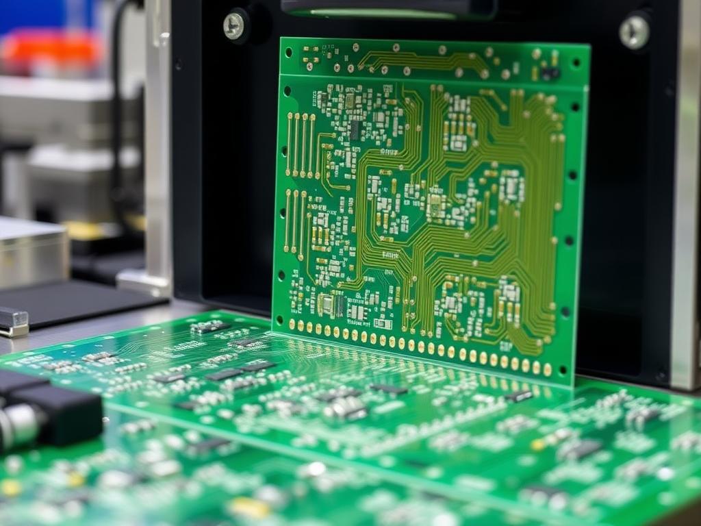
디패널링 is the final step in PCB 조립, where individual 회로 기판 are separated from the larger panel they were manufactured on. The traditional methods for separating PCBs는, like using saws and routers, can introduce 기계적 응력, create dust, and generate waste. It’s a process often overlooked, but it plays a vital role in the overall environmental impact of PCB manufacturing and assembly. More efficient and environmentally friendly depaneling techniques are now available, helping to move towards more sustainable manufacturing options. By optimizing this step, we can reduce waste and improve the ecological impact of our industry, making pcbs are green in the process.
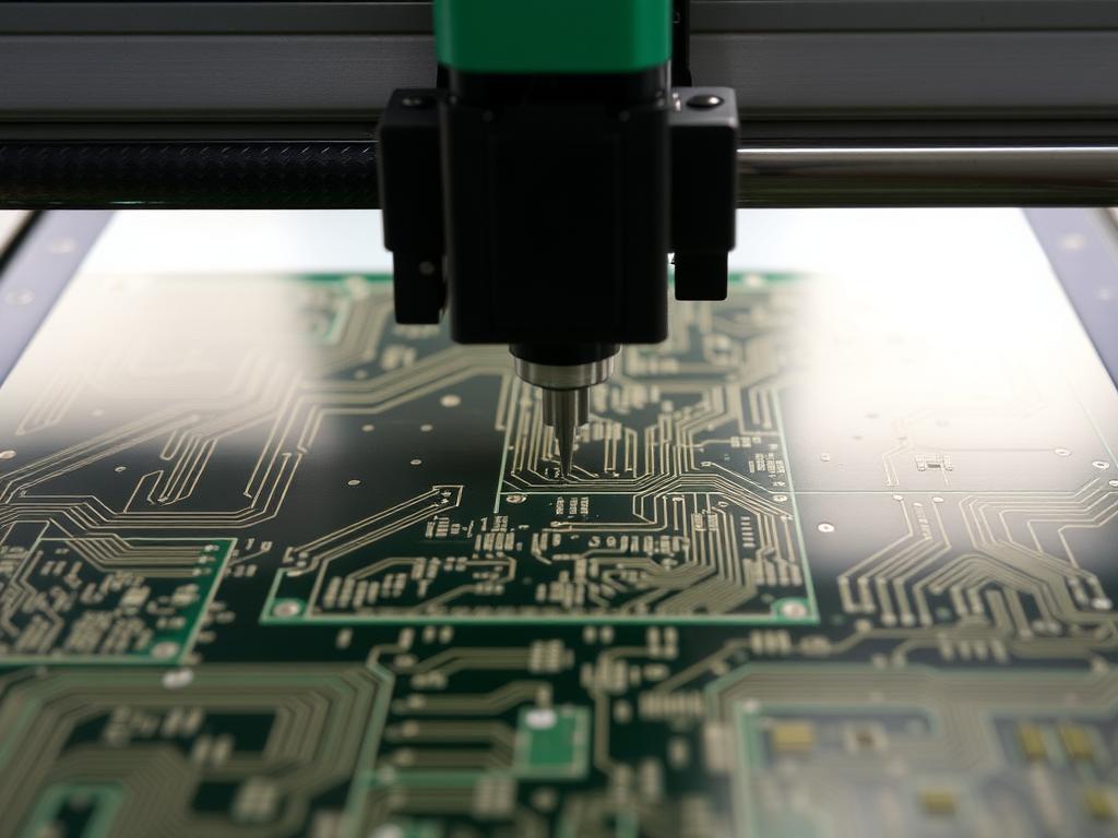
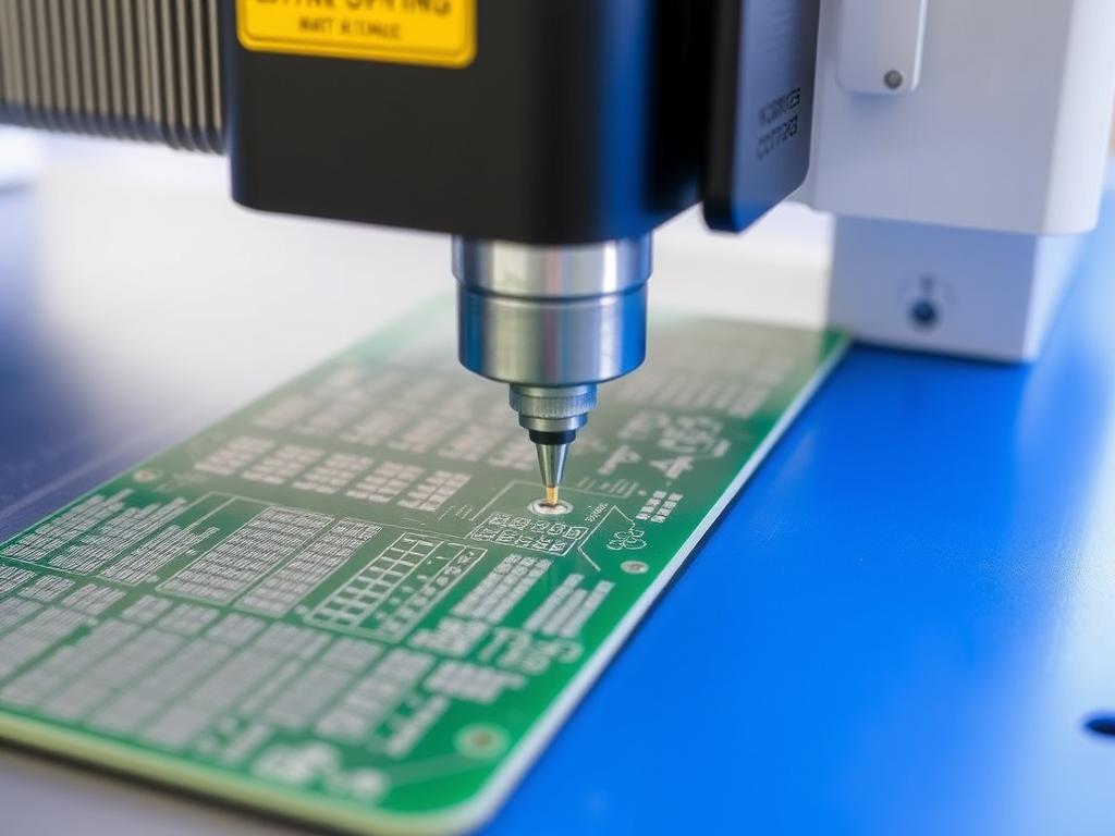
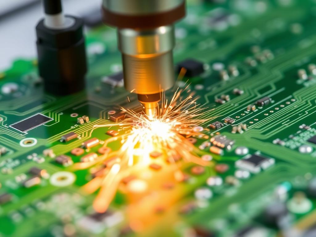
How Do Laser Systems Contribute to Eco-Friendly PCB Manufacturing?
레이저 기술 혁명을 일으켰다 pcb 디패널링. Unlike traditional mechanical methods, 레이저 시스템 제공하다 비접촉 cutting process. This means minimal material waste, no dust generation, and significantly reduced 기계적 응력 에 회로기판. 레이저 디패널링 is not only more precise but also more environmentally friendly, reducing reliance on chemical solutions and the need for frequent tool changes, contributing to a reduction in environmental impact. The move to 원자 램프 based processes aligns with adopting green production methods, and for me, after 20 years, it’s like watching the future unfold right before your eyes.
What are the Advantages of Laser Depaneling Over Traditional Methods?
그것에 관해서 pcb 디패널링, traditional methods like routing and sawing can be messy and imprecise. They often lead to material waste and can potentially damage the 회로. 와 함께 레이저 디패널링, we achieve much higher precision with a clean cut and minimal environmental effects. The precision of the 레이저 빔 ensures that even delicate boards are separated cleanly and safely, thereby improving operational efficiency, and reducing overall material consumption. We all know that means both cost and environmental benefits in the long run.
How Can PCB Manufacturers Reduce Waste in the Depaneling Process?
Reducing waste is critical in the PCB 제조 공정. By switching to precision methods such as laser cutting, we reduce waste dramatically. And with modern 레이저 디패널링 기계, 그 분리 방법 panels is more precise than ever, resulting in less wasted material. We also encourage the use of recyclable materials wherever possible, and we actively promote recycling programs to ensure that waste is handled responsibly. For me, it’s not just about making high-quality PCBs, it’s also about leaving a smaller ecological footprint.
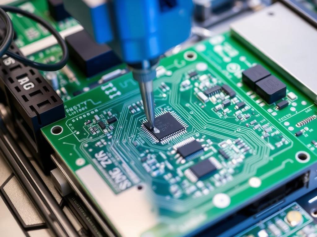
What Role Does Automation Play in Sustainable PCB Production?
오토메이션 is paramount in achieving sustainable manufacturing. 자동화됨 디패널링 기계, like our GAM series, are designed to improve operational efficiency, reduce manual handling, and ensure consistent output with minimal waste. The integration of 머신 비전 further enhances accuracy by inspecting each board before and during the 디패널링 process. This increases the quality of pcb 조립 and helps us optimize material usage, contributing to our commitment to sustainability. We use these kinds of advances to constantly improve our 제조 공정.
How Does Material Selection Affect the Environmental Impact of PCBs?
The choice of materials used to manufacture 회로 기판 has a significant impact on the environment. We’re moving away from hazardous substances and promoting the use of eco-friendly alternatives. Where possible, we’re exploring biodegradable 또는 recyclable substrates and ensuring that our processes comply with RoHS (Restriction of Hazardous Substances) standards. We also focus on the responsible use of resources like copper and aluminum, minimizing the demand for new resources, and ensuring that our pcb substrates are more environmentally friendly.
What Are the Long-Term Benefits of Implementing Sustainable Practices?
Implementing sustainable manufacturing methods offers significant long-term benefits for all stakeholders. For pcb manufacturers, this means not only meeting environmental regulations but also enhancing operational efficiency and reducing long-term costs. For our customers, this translates to access to high-quality, environmentally friendly PCBs는, bolstering their brand image and increasing consumer confidence. Additionally, our commitment to sustainability contributes to a healthier planet by reducing overall pollution and promoting the responsible use of resources.
What are Some Specific Examples of Sustainable PCB Manufacturing Methods?
Besides 레이저 디패널링, we focus on several other sustainable practices, such as the efficient use of water and energy during the pcb manufacturing process. We prioritize the use of 무연 솔더 and minimize the use of volatile organic compounds in our processes. Our entire approach is geared towards reducing environmental damage and optimizing our production processes for greater efficiency. This includes adopting a “cradle-to-cradle” approach that maximizes the recycling of materials, helping to move towards a more circular economy within the 전자 산업.
Why Should You Choose Our Sustainable Depaneling Solutions?
20년의 경험을 바탕으로 PCB 제조 industry, I’ve personally overseen the development of advanced and sustainable depaneling 솔루션. 우리의 디패널링 기계 are the product of years of refinement, designed to meet the most stringent environmental regulations and deliver consistent, high-quality results. Trusted by industry leaders like TP-LINK, Canon, BYD, and Foxconn, our technology is proven, reliable, and effective. We’re not just selling equipment; we’re offering a partnership to help you achieve your sustainability goals, while enhancing the quality of your products and contributing to the shift towards sustainability. 문의하기 today for a free quote, and let us help you move towards a greener, more sustainable future.
자주 묻는 질문
What are the main differences between laser and traditional depaneling methods? Laser depaneling offers more precision, less waste, and reduces mechanical stress, compared to traditional methods like routing which often create dust and potential damage.
How does using green materials in PCB production benefit the environment? Using green materials and processes helps reduce waste, minimizes the use of hazardous substances, and leads to a smaller environmental footprint during the manufacturing of printed circuit boards, protecting human health and our ecosystem.
Is laser depaneling more expensive than traditional methods? While the initial investment may be higher, laser depaneling can lead to significant long-term savings due to reduced material waste, improved precision, and lower maintenance costs, ultimately making it a cost-effective solution.
What types of sustainability standards do you adhere to in your manufacturing? We adhere to strict sustainability standards including ISO 14001, RoHS, and other relevant environmental standards, focusing on reducing pollution, conserving resources, and minimizing waste.
Can implementing sustainable practices improve our company’s brand image? Absolutely! By showcasing a commitment to sustainability, you not only enhance your brand’s reputation but also attract customers who prioritize environmental management and responsible manufacturing.
주요 내용:
- Sustainable practices are not just an ethical choice, but a business imperative for the 전자 산업.
- 레이저 디패널링 offers significant environmental benefits compared to traditional methods.
- 오토메이션 is crucial for achieving efficiency and reducing waste in PCB 생산.
- Material selection plays a critical role in minimizing the environmental impact of PCB manufacturing.
- We have years of experience in pcb 제조 and offer trusted, reliable solutions from pcb 라우터 머신 에게 PCB 레이저 디패널링.
- Our commitment to sustainability can help you meet regulatory requirements and improve your brand’s image, and help make pcbs are green.
- By adopting sustainable electronics manufacturing, we’re not just creating better PCBs는, we’re also building a better future for everyone.
내부 링크:
- For more on our advanced depaneling solutions, visit our PCB 라우터 기계 페이지.
- Explore our range of environmentally friendly V-홈 디패널링 옵션.
- Learn more about our automated solutions at our 자동장비 페이지.
- See how our PCB/FPC 펀칭기 can improve your manufacturing.
- Browse our selection of 부속품 to optimize your production line.
- Discover how our SMT 전체 라인 장비 can enhance your operations.