![]()

European PCB depaneling solutions
Precision Laser PCB Depaneling Solutions: Revolutionizing SMT and Electronics Manufacturing
In today’s fast-paced electronics manufacturing landscape, achieving 정밀한 and efficient pcb 디패널링 is paramount. As someone deeply entrenched in this industry for over two decades, I’ve witnessed firsthand the evolution from traditional methods to the sophisticated 원자 램프 solutions we utilize today. This article will delve into the world of pcb 디패널링, particularly focusing on the transformative power of 레이저 디패널링, and why choosing the right 디패널링 머신 is crucial for your 조작 success. Understanding these nuances can significantly impact your production line, and that’s why this deep dive is essential for anyone involved in electronics assembly.
Article Outline: Exploring the Landscape of PCB Depaneling
Here’s a detailed roadmap of what we’ll cover in this comprehensive guide to pcb 디패널링:
What is PCB Depaneling and Why Does Precision Matter in Circuit Board Separation?
Why Choose Laser Depaneling Over Mechanical Methods for Your PCBs?
What Types of PCB Depaneling Machines Are Available: Routers, V-Cuts, and Punches?
How Does Laser Depaneling Ensure Precise Separation Without Mechanical Stress on Sensitive Components?
What are the Key Advantages of Laser PCB Depaneling for High-Quality Circuit Boards?
What Factors Should You Consider When Choosing a PCB Depaneling Solution for Your Production Line?
What Industries Benefit Most from Advanced PCB Laser Depaneling and High-Volume Production?
How Can Automatic Equipment and Inline Systems Optimize Your Depaneling Process?
What Accessories and SMT Whole Line Equipment Complement Efficient PCB Depaneling?
Ready to Optimize Your PCB Depaneling with Our Expert Solutions?
What is PCB Depaneling and Why Does Precision Matter in Circuit Board Separation?
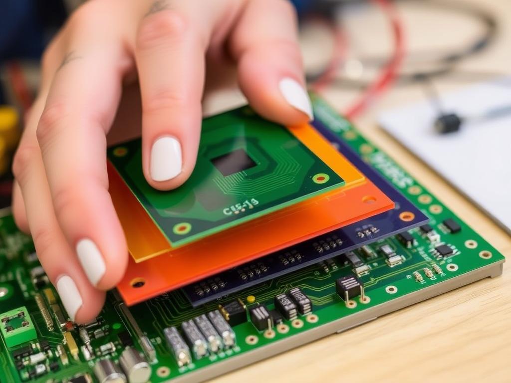
PCB 디패널링 이다 프로세스 of separating individual PCBs는 더 큰 것에서 패널 후에 구성 요소 have been assembled. Think of it like separating squares of a chocolate bar after it’s been made. The crucial element here is 정도. For years, I’ve seen the headaches caused by imprecise 분리. Cracked boards, damaged 구성 요소, and ultimately, increased scrap rates. 정밀한 디패널링 ensures that each individual 회로기판 is perfectly separated without inducing any 기계적 응력 에 민감한 구성 요소. This is critical for the reliability and longevity of the final 전자 product. Poorly executed 디패널링 can lead to micro-fractures that might not be immediately apparent but can cause failures down the line, a costly problem for any 제조업체.
The evolution of 디패널링 methods reflects the increasing demands for 정확성 and efficiency in the electronics 산업. Early methods were often manual and prone to errors. Now, we have sophisticated 시스템 좋다 레이저 디패널링 기계 that offer unparalleled 정도. This shift is driven by the miniaturization of electronics and the increasing density of 구성 요소 ~에 PCBs는. The margin for error has shrunk dramatically, making 정밀한 디패널링 not just a preference, but a necessity.
Why Choose Laser Depaneling Over Mechanical Methods for Your PCBs?
For many years, 기계적인 다음과 같은 방법 pcb routing, V컷, 그리고 펀치 methods were the standard for 디패널링. While these methods still have their place, 레이저 디패널링 has emerged as a superior 해결책 for many applications, especially where 정도 is paramount. As a leading supplier of 디패널링 기계, we’ve seen the transformative impact of 원자 램프 기술.
Here’s why 레이저 디패널링 often outshines traditional approaches:
- 뛰어난 정밀도: 레이저 커팅 offers exceptional 정확성, allowing for complex and intricate 절단 paths that 기계적인 methods struggle with. This is especially important for PCBs는 밀접하게 배치된 구성 요소.
- 감소된 기계적 스트레스: Unlike 라우터 또는 V컷 기계, 레이저 디패널링 비접촉식이다 프로세스, eliminating the 기계적 응력 that can damage 민감한 구성 요소. This is a game-changer for delicate PCBs는.
- 유연성: 레이저 시스템 can handle a wide range ~의 피씨비 materials and thicknesses with simple 프로그램 adjustments, offering greater 유연성 in your 생산.
- 깨끗한 컷: 레이저 디패널링 produces clean and smooth edges, minimizing 먼지 and debris, which is crucial for maintaining a clean 조작 환경.
- Intricate Designs: 원자 램프 technology allows for the 분리 ~의 PCBs는 with complex shapes and internal cutouts that are difficult or impossible to achieve with 기계적인 행동 양식.
While initial investment in 레이저 디패널링 equipment might be higher, the long-term benefits, including reduced scrap rates, improved product reliability, and greater design 유연성, often make it a more cost-effective 해결책 in the long run.
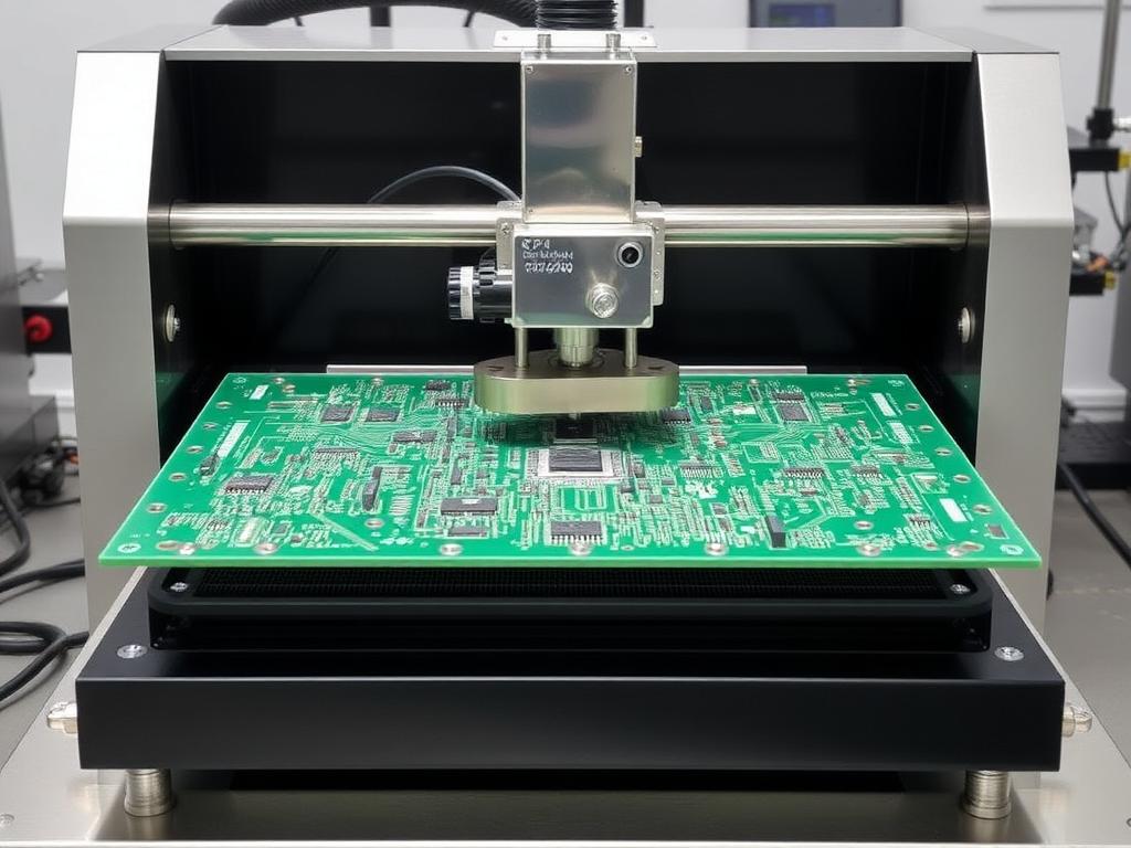
What Types of PCB Depaneling Machines Are Available: Routers, V-Cuts, and Punches?
세계의 pcb 디패널링 offers a diverse range of 기계, each with its strengths and weaknesses. Understanding these differences is key to selecting the right equipment for your specific needs. From my experience, a wide range of options ensures that there’s a suitable 해결책 for every 제조 공정.
Here’s a brief overview of the common types:
- PCB 라우터 머신: 이것들 기계, like our popular GAM 380AT PCB 바닥 디패널링 기계, utilize a rotating 커터 에게 분리된 그만큼 PCBs는. They are versatile and can handle various 피씨비 thicknesses. Our PCB 라우터 기계 category also highlights the broader applications of this technology.
- V-Groove 디패널링 기계: 이것들 기계 use blades to score a “V” groove on both sides of the 피씨비 along the separation line. The PCBs는 are then snapped apart. Our selection of V-홈 디패널링 solutions caters to different production volumes.
- PCB/FPC Punching Machines: 이것들 기계, exemplified by our ZM10T & 15T PCB & FPC 펀칭 절단기, use a die and punch to 분리된 그만큼 PCBs는. They are ideal for high-volume production of PCBs는 with simple shapes.
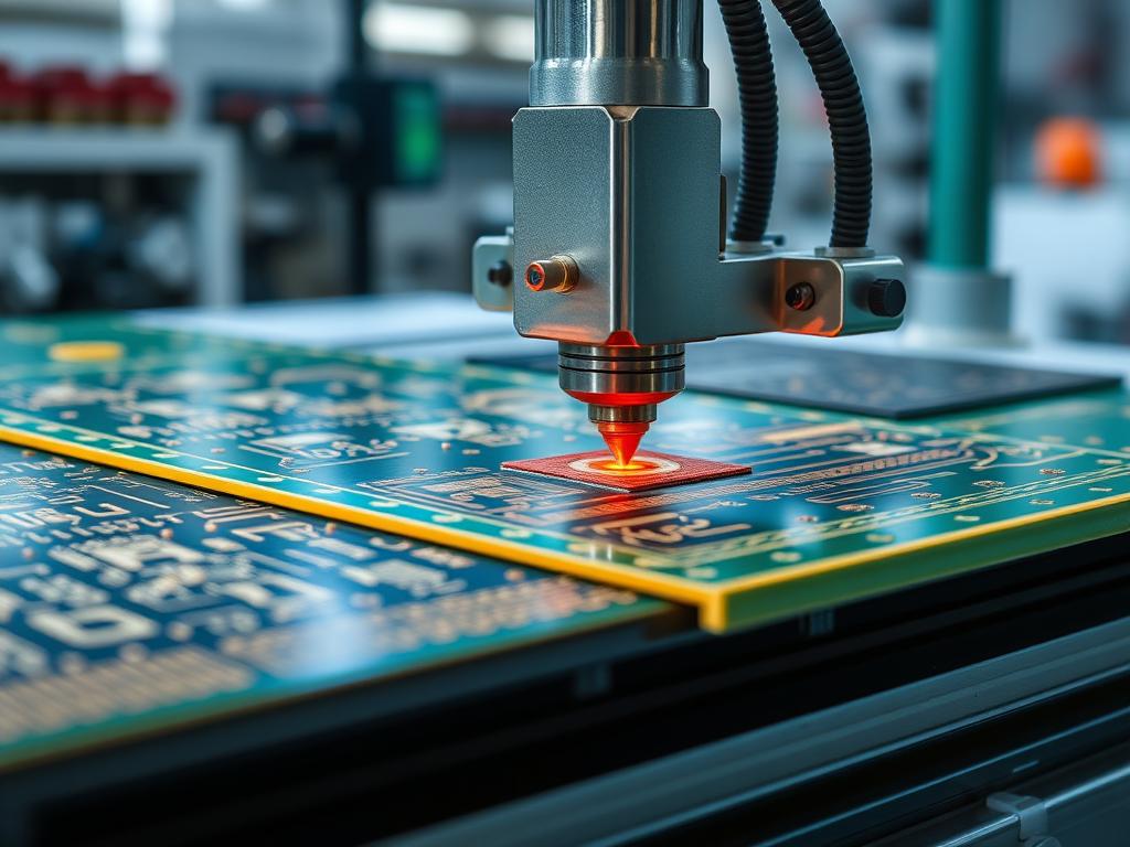
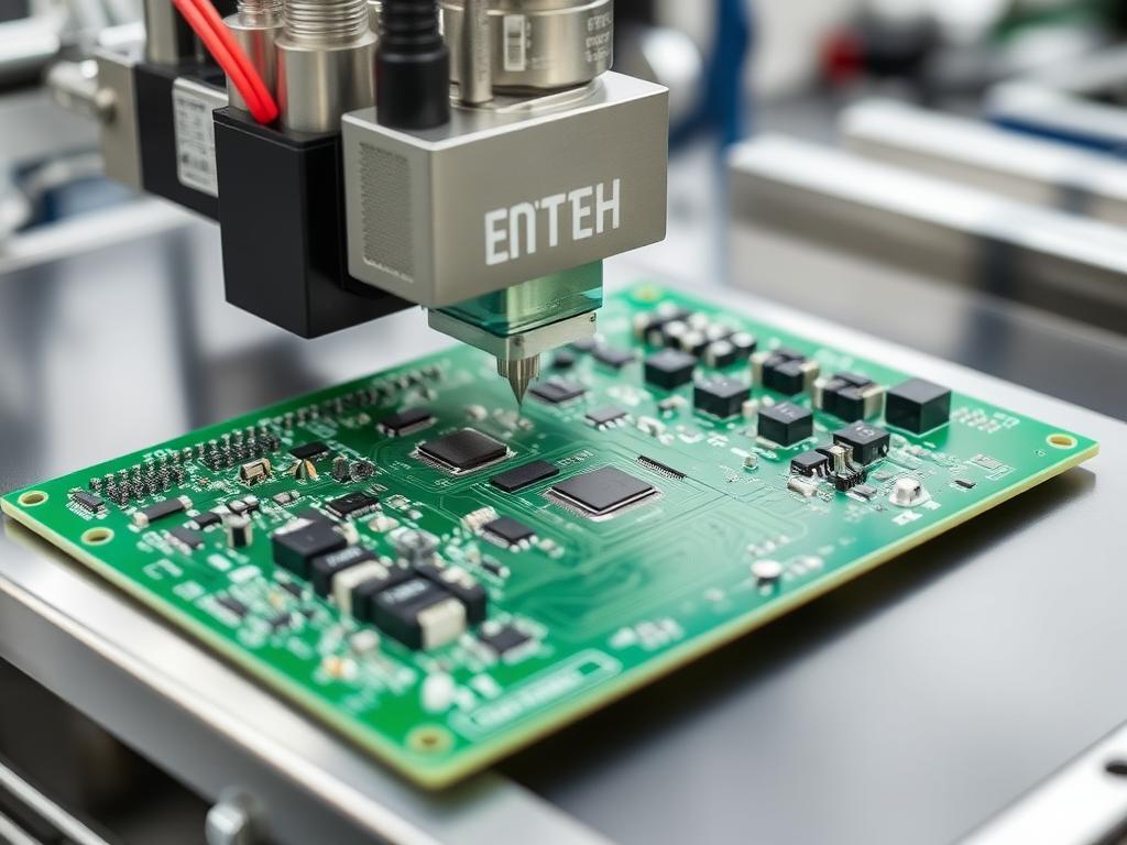
- 레이저 디패널링 기계: As discussed, these 기계, 우리의 것과 같은 DirectLaser H5 PCB-FPC 레이저 커팅 머신, employ a 레이저 소스 to precisely cut through the 피씨비. They offer unmatched 정도 and minimal stress. Explore our dedicated PCB 레이저 디패널링 section for more information.
선택의 디패널링 머신 depends on factors like production volume, 피씨비 design complexity, material, and budget.
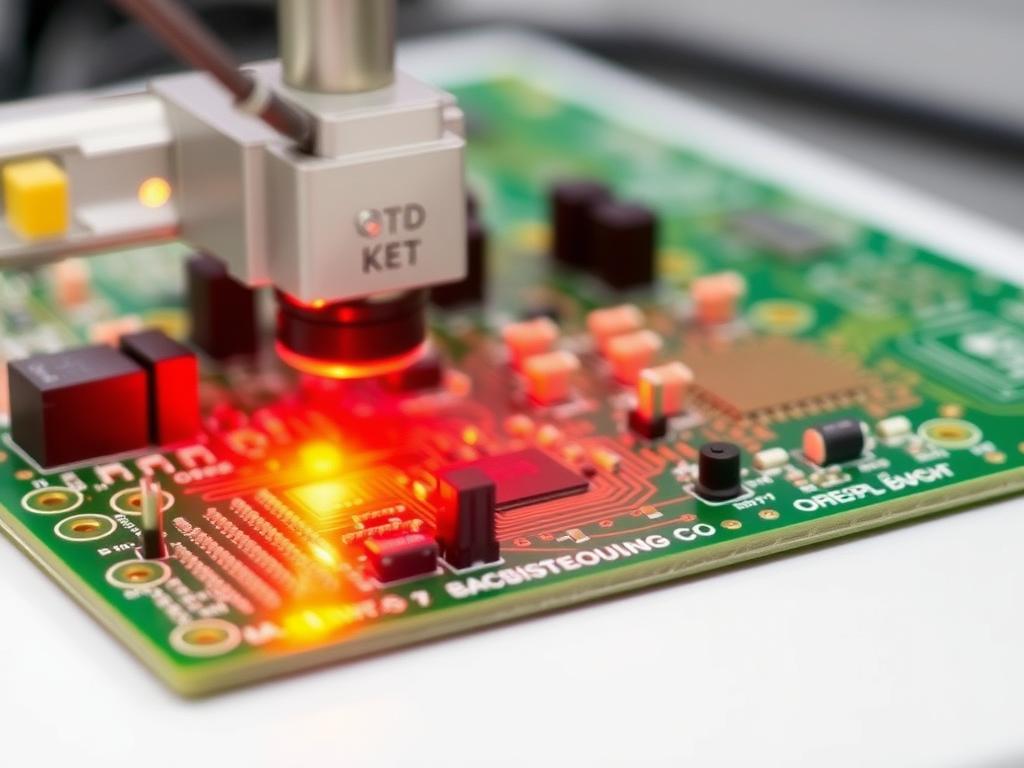
How Does Laser Depaneling Ensure Precise Separation Without Mechanical Stress on Sensitive Components?
The beauty of 레이저 디패널링 lies in its non-contact nature. Unlike 기계적인 methods that involve physical force, 레이저 디패널링 uses a highly focused beam of light to vaporize the 피씨비 material along the desired cutting path. This fundamental difference is what allows for precise separation without inducing 기계적 응력.
Imagine trying to 분리된 delicate glass – you wouldn’t want to use a saw, would you? The same principle applies to PCBs는 ~와 함께 민감한 구성 요소. 그 원자 램프 beam, precisely controlled in terms of power and movement, effectively “melts” away the material, leaving a clean and smooth edge. This minimizes the risk of damaging delicate 구성 요소 or creating micro-fractures in the 판자.
Furthermore, advanced 레이저 디패널링 시스템 often incorporate features like 자외선 lasers, which further reduce heat-affected zones, ensuring even greater protection for 민감한 구성 요소. 그 정확성 의 원자 램프 beam, often measured in microns, allows for intricate cuts and tight tolerances, making it ideal for modern, densely populated PCBs는. 이것 precise separation without physical contact is a significant advantage, especially in industries where component integrity is paramount.
What are the Key Advantages of Laser PCB Depaneling for High-Quality Circuit Boards?
For over 20 years, I’ve championed the adoption of technologies that elevate 조작 standards. 레이저 디패널링 is undoubtedly one of those technologies. Its advantages extend beyond just 정도 and touch upon several critical aspects of pcb 생산:
- High Accuracy and Repeatability: 레이저 시스템 offer exceptional 정확성 and repeatability, ensuring consistent and high-quality 분리 across the entire 생산 run. This 정확성 minimizes scrap and rework.
- Minimal Material Waste: 그만큼 정밀한 의 본질 레이저 커팅 minimizes material waste compared to some 기계적인 methods, leading to cost savings and a more sustainable 제조 공정.
- Processing of Complex Shapes: 레이저 디패널링 excels at handling PCBs는 with complex contours, internal cutouts, and intricate designs that are challenging for traditional methods.
- 감소된 툴링 비용: Unlike 펀칭 머신 that require custom dies, 레이저 시스템 are highly programmable, eliminating the need for expensive and time-consuming tooling changes.
- Improved Edge Quality: 레이저 커팅 produces clean, smooth edges free from burrs or irregularities, improving the overall quality and aesthetics of the 인쇄 회로.
- Suitable for a Wide Range of Materials: 레이저 디패널링 can effectively process various 피씨비 materials, including FR4, flex PCBs는, and metal-core PCBs는, offering greater versatility.
These advantages collectively contribute to higher quality 회로 기판, reduced 생산 costs, and increased efficiency, making 레이저 디패널링 a compelling choice for modern electronics 조작.
What Factors Should You Consider When Choosing a PCB Depaneling Solution for Your Production Line?
올바른 것을 선택하기 pcb depaneling solution 귀하에게 상당한 영향을 미칠 수 있는 중요한 결정입니다. 생산 efficiency and product quality. Having guided countless companies through this process, I’ve identified several key factors to consider:
- 생산량: 대용량의 경우 생산, 완전 자동화 인라인 시스템 우리처럼 GAM 360AT 인라인 PCB 분리기 are essential. For lower volumes, offline or semi-automatic 기계 might be more suitable.
- PCB Design and Complexity: 복잡한 피씨비 shapes and the presence of 민감한 구성 요소 often necessitate the 정도 ~의 레이저 디패널링. Simpler designs might be adequately handled by V컷 또는 펀치 행동 양식.
- Material Type and Thickness: Consider the materials you’re working with. 레이저 시스템 권하다 유연성 across various materials, while 기계적인 methods might have limitations.
- Budget and ROI: Evaluate the initial investment and the long-term return on investment. While laser machines can have a higher upfront cost, the benefits in terms of reduced scrap and improved quality can lead to significant savings.
- 자동화 요구 사항: Do you need a standalone 기계 또는 완전 자동화 인라인 체계 that integrates with your existing 생산라인? 우리의 자동장비 category provides insights into these solutions.
- 유지 보수 및 지원: Consider the availability of maintenance services and technical support. A reliable provider is crucial for ensuring continuous operation.
- Footprint and Space Requirements: Evaluate the physical space available in your 조작 facility.
Careful consideration of these factors will help you choose the 디패널링 솔루션 that best aligns with your specific needs and optimize your 제조 공정.
What Industries Benefit Most from Advanced PCB Laser Depaneling and High-Volume Production?
The benefits of advanced pcb laser depaneling are far-reaching, impacting a multitude of industries that rely on high-quality and reliable electronic products. From my extensive experience, several sectors stand out as prime beneficiaries:
- 가전제품: Companies like TP-LINK, Xiaomi, and OPPO (all our valued customers) demand 정밀한 and efficient 디패널링 for their smartphones, tablets, and other consumer devices. High-volume 생산 with minimal defects is critical in this sector.
- 자동차: The automotive industry relies heavily on complex electronic control units (ECUs). 레이저 디패널링 ensures the integrity of these critical components, contributing to vehicle safety and reliability. BYD, another of our esteemed clients, understands this imperative.
- 의료 기기: In the medical field, precision and reliability are paramount. 레이저 디패널링 is ideal for separating PCBs는 used in life-saving equipment, ensuring the highest quality standards.
- 통신: Companies like Lenovo and HONOR require robust and reliable electronic components in their networking and communication equipment. 정밀한 디패널링 is essential for ensuring the performance of these products.
- Aerospace and Defense: The stringent requirements of the aerospace and defense industries necessitate the highest levels of 정도 and reliability. 레이저 디패널링 plays a crucial role in manufacturing mission-critical electronic systems.
- Industrial Automation: Industrial control systems demand robust and dependable electronics. 레이저 디패널링 contributes to the longevity and reliability of these systems in demanding environments.
The demand for 고품질 electronics across these industries makes advanced pcb laser depaneling an indispensable technology for maintaining competitiveness and ensuring product excellence.
How Can Automatic Equipment and Inline Systems Optimize Your Depaneling Process?
In today’s high-throughput 조작 environments, 오토메이션 최대화하는 것이 핵심입니다 능률 and minimizing errors. Integrating 자동 장비 그리고 인라인 시스템 당신의 디패널링 프로세스 can bring significant advantages.
Automatic depaneling machines, 우리의 것과 같은 GAM 336AT 인라인 자동 PCB 디패널링 기계, can operate continuously with minimal human intervention, significantly reducing cycle time and labor costs. Inline systems seamlessly integrate the 디패널링 stage into the broader SMT 전체 라인 장비, creating a continuous flow of PCBs는 를 통해 생산 process. This reduces 손질, minimizes the risk of damage, and improves overall throughput.
뿐만 아니라, 자동 장비 can incorporate features like automatic loading and unloading of pcb 패널, as well as sophisticated vision 시스템 for precise alignment and quality control. Our 자동장비 range showcases solutions like the GAM 630V 자동 분류 및 팔레타이징 기계, further streamlining the post-depaneling handling. By automating the 디패널링 프로세스, manufacturers can achieve higher levels of 능률, consistency, and product quality.
What Accessories and SMT Whole Line Equipment Complement Efficient PCB Depaneling?
To achieve optimal 능률 and performance in your pcb 디패널링 operation, it’s essential to consider the complementary 부속품 그리고 SMT 전체 라인 장비. These components can significantly enhance the overall 프로세스.
을 위한 pcb 라우터 기계, having a supply of high-quality 밀링 커터 is crucial for maintaining cutting 정확성 and extending tool life. For 레이저 디패널링 시스템, proper fume extraction 시스템 are necessary to remove dust and debris, ensuring a clean and safe working environment.
Integrating your 디패널링 머신 into the broader SMT 전체 라인 장비 is also vital for a seamless 생산 flow. This can include conveyor 시스템 for transferring PCBs는 between stations, loading and unloading equipment, and inspection 시스템 에게 보장하다 quality. Our expertise extends to providing SMT In-Line Depaneling Machine Solutions, ensuring seamless integration with your existing 생산라인. Considering these 부속품 그리고 전체적으로 SMT line integration is crucial for maximizing the 능률 and effectiveness of your pcb 디패널링 프로세스.
Ready to Optimize Your PCB Depaneling with Our Expert Solutions?
With over 20 years of experience in the pcb 디패널링 산업, we at pcbdepaneling.com understand the critical role that 정밀한 and efficient 분리 plays in your 조작 success. Our wide range ~의 디패널링 기계, 에서 고정밀 레이저 시스템 to robust 라우터 그리고 V컷 options, are designed to meet the diverse needs of electronic technology companies and 피씨비 players worldwide.
Trusted by industry leaders like TP-LINK, Canon, BYD, Flex, TCL, Xiaomi, Lenovo, OPPO, HONOR, and Foxconn, our 디패널링 솔루션 are proven to deliver outstanding performance and 신뢰할 수 있음. Whether you’re seeking a standalone 기계 또는 완전 자동화 인라인 체계, we have the expertise and the technology to optimize your 디패널링 프로세스.
비효율적이지 않도록 하세요 디패널링 hold back your 생산. Contact us today to discuss your specific requirements and discover how our cutting-edge pcb 디패널링 기계 can elevate your 조작 능력.
PCB 디패널링에 대한 자주 묻는 질문
차이점은 무엇입니까? pcb routing 그리고 레이저 디패널링? PCB 라우팅 uses a mechanical 커터 에게 분리된 PCBs는, 하는 동안 레이저 디패널링 를 사용합니다 원자 램프 beam. 레이저 디패널링 더 높은 것을 제공합니다 정도 and less 기계적 응력.
~이다 레이저 디패널링 suitable for all types of PCBs는? 레이저 디패널링 is highly versatile and suitable for a wide range ~의 피씨비 materials and thicknesses, including FR4, flex PCBs는, and metal-core PCBs는.
사용의 이점은 무엇입니까? automatic depaneling machine? Automatic depaneling machines increase 능률, reduce labor costs, improve consistency, and minimize the risk of human error.
어떻게 올바른 것을 선택합니까? pcb 디패널링 머신 for my needs? Consider your production volume, 피씨비 design complexity, material type, budget, and automation requirements.
Do you offer support and maintenance for your 디패널링 기계? Yes, we provide comprehensive support and maintenance services for all our 디패널링 기계.
효율적인 PCB 디패널링을 위한 주요 사항
- 정도 가장 중요하다 pcb 디패널링 to avoid damaging 민감한 구성 요소.
- 레이저 디패널링 offers superior 정확성 and minimizes 기계적 응력.
- 에이 wide range ~의 디패널링 기계 are available, including 라우터, V컷 기계, 펀칭 머신, 그리고 레이저 시스템.
- 올바른 것을 선택하다 디패널링 솔루션 귀하의 특정 사항에 따라 달라집니다 생산 needs and 피씨비 형질.
- Automatic equipment 그리고 inline systems can significantly optimize your 디패널링 프로세스.
- 적절한 부속품 and integration with SMT 전체 라인 장비 enhance 능률.
By understanding these key aspects of pcb 디패널링, you can make informed decisions to optimize your 제조 공정 and ensure the highest quality for your electronic products.