![]()

Safety precautions in PCB depaneling
PCB Depaneling: Mastering the Art of Separating Printed Circuit Boards
For over two decades, I’ve been deeply involved in the PCB industry, witnessing firsthand the evolution of PCB depaneling techniques. This article is a culmination of that experience, designed to guide electronic technology companies, large electronic product processing factories, and individual PCB enthusiasts through the crucial process of separating printed circuit boards (PCBs) from their manufacturing panels. We’ll explore everything from the fundamental rules for handling printed circuit boards to the latest in лазерлік депанельдеу, ensuring that your ПХД are treated with the care they deserve. Whether you’re dealing with standard FR-4 ПХД or more complex flexible circuits, understanding the nuances of депанелизация is paramount to maintaining quality and minimizing losses. It’s a journey through best practices and innovative technologies, aiming to equip you with the knowledge to choose the perfect депанелизация method for your needs.
What is PCB Depaneling and Why is it Crucial?
The term “депанелизация” refers to the process of separating individual PCbs кейін үлкенірек панельден өндірістік процесс. This step is absolutely critical in the production of electronics. When creating ПХД, it’s far more efficient to manufacture several circuit boards at once on a single large panel. This process, called панелизация, allows for higher өткізу қабілеті and reduces waste. Once the board built using various layers of material is complete, the individual PCBs must be separated. This is where the art and science of депанелизация come in. Incorrect депанелизация can lead to a whole host of problems, such as cracked traces, damaged components, and even complete board failure. Депанельдеу needs to be done with care and with the correct type of equipment. This is not just a simple бөлу процесі, it’s a vital step that impacts the overall integrity and functionality of the final product.
The way you choose to perform депанелизация has a direct impact on the success of your products. Choosing the incorrect кесу әдісі can cause damage and result in a disappointing loss. Poor депанелизация can introduce механикалық кернеу and other forms of stress to sensitive areas, like электрондық компоненттер, and can lead to functional failures. It’s not simply about cutting a PCB apart; it’s about ensuring each individual pcb is perfectly usable when separated. The methods used for PCB депанельдеу are varied, with some being more suitable than others based on type of pcb, materials, and precision needs. Thus, understanding the options and choosing the right one for your needs is a step every manufacturing team must take with greatest of care.
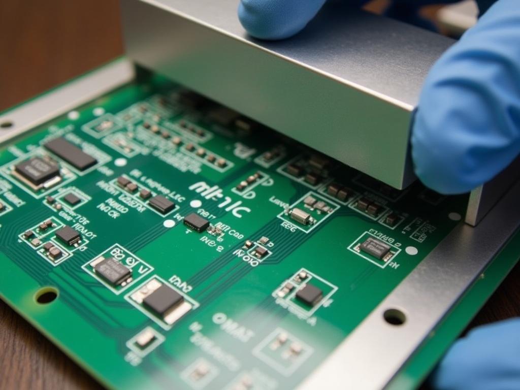
Why is Proper Handling of Printed Circuit Boards So Important?
As someone who has spent two decades in this field, I’ve seen the results of mishandling countless times. Printed circuit boards are delicate and must be handled бірге the greatest of care. They are full of sensitive electronic components that are easily damaged. A pcb can fracture with just a bit of too much bending or twisting, so it needs to be treated as the critical piece of equipment that it is. A cracked trace or a damaged capacitor can render a circuit board goes from being functional to being scrap with just a moment of carelessness. This isn’t just about cause damage to the actual PCB, but also about the risk of contamination and electrostatic damage.
Proper handling is not just about avoiding physical damage. It’s also about preventing the introduction of contaminant, and making sure that electrostatic discharge (ESD) is kept to a minimum. Imagine your PCbs as a finely tuned machine: if something gets out of place or too much pressure is put on a specific part, the entire thing falls apart. It is paramount that appropriate protective clothing like wrist straps connected to ground are worn at all times, and that we follow the rules for handling printed circuit boards. Many times there is a lot of handling involved in the тазарту процесі and the pick-and-place and general SMT areas of the production process. These steps are crucial in ensuring that your PCbs go from being built to being ready for their intended use.
What are the Key Design Rules for PCB Panelization?
Тиімді panel design is absolutely crucial for successful депанелизация. The way a panel is created significantly impacts how easily the жеке компьютерлер can be separated. One of the first things to consider is the size of the panel, the number of PCbs per panel, және material thicknesses. You have to take into account the size of your PCB, and the size of the machines that you are using.
When you think about PCB дизайны үшін панелизация, it’s not only about how many PCbs you can fit, it’s about maximizing utilization of the panel, while making sure it is still easy to perform the кесу процесі without cause damage. The spacing between PCbs, the width of the cutting channel, the location of fiducial marks, and the placement of tooling holes are also vital considerations. You want to ensure you have enough free areas for handling and that there are no components close to the edges that might be damaged during separation. Remember, panel design influences not only the тазарту процесі but also the efficiency of the pick-and-place operations. The better the panel design, the less механикалық кернеу there will be and more consistent the end result.
What Depaneling Methods are Available?
Бірнеше бар тазарту әдістері, and each method has its advantages and disadvantages. The method you choose should be based on the type of pcb you’re using, the volume of production, the precision requirements, and the budget that you have. Here are some common депанелизация approaches:
- Router Depaneling: A mechanical method using a high-speed spindle to cut through the material.
- Лазерлік депанельдеу: Utilizes a focused laser beam to cut through the material.
- V-groove депанельдеу: Uses a v-scoring or v-кесу method, where grooves are pre-scored before the boards are broken apart.
- Punching Depaneling: A method using a die to punch out the individual PCbs.
Each of these тазарту әдістері has a different approach, and that leads to different outcomes. Understanding these methods is the key to choosing the best way to separate your PCbs.
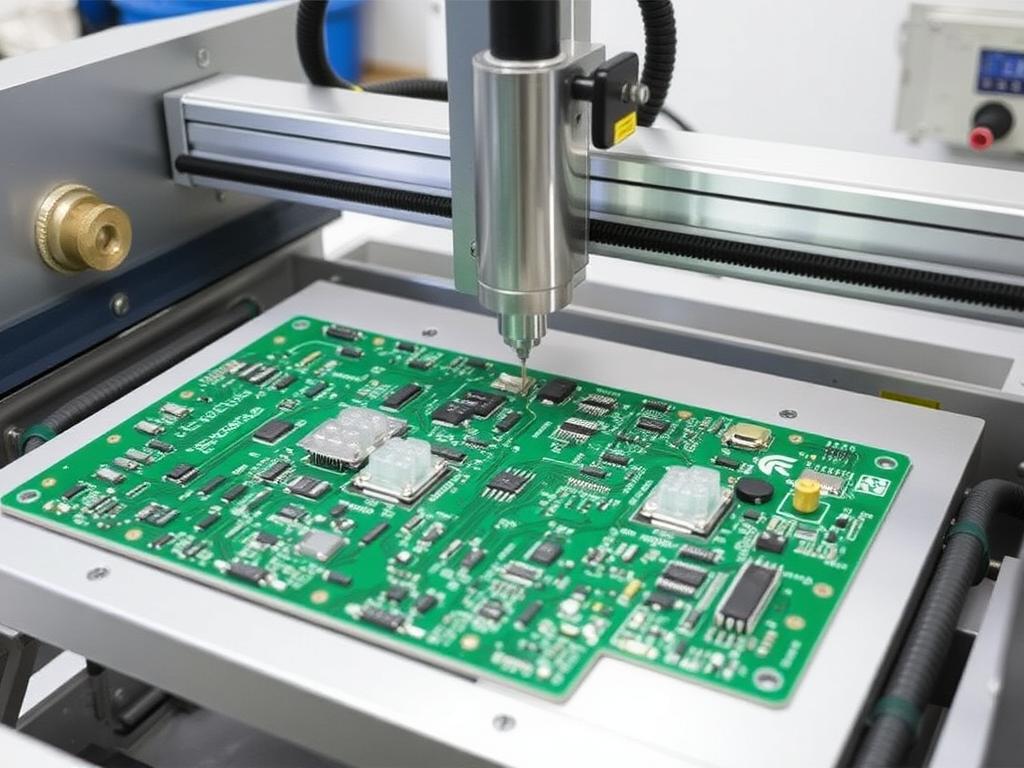
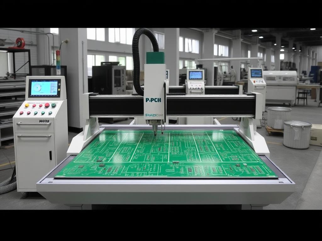
How Does Router Depaneling Work and When Should You Choose it?
Router depaneling болып табылады widespread method that uses a high-speed rotary cutter, or маршрутизатор, to separate жеке компьютерлер from the panel. This method is versatile and can be used on a wide variety of PCB materials and thicknesses. The маршрутизатор moves along a pre-programmed path, essentially milling away the субстрат and separating the boards.
The benefits of router depaneling include its ability to handle complex shapes, to create a clean edge with less механикалық кернеу than other methods, and its flexibility when it comes to complex contours. However, router depaneling does create dust and debris, requiring a thorough cleaning process after separation, which impacts technical cleanliness. Бұл кесу әдісі is ideal for moderate to high-volume PCB production runs where a clean edge and precise cuts are required. It is also a great option for PCbs that have сезімтал компоненттер close to the edge, as long as the appropriate settings are used. We are known as a leading manufacturer of PCB маршрутизаторы, and we are confident in our products.
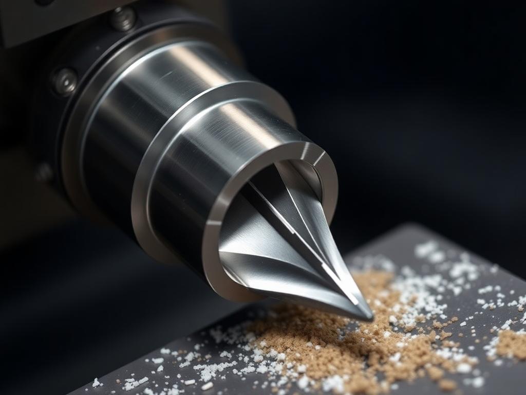
What is Laser Depaneling and When is it the Best Option?
Лазерлік депанельдеу is a non-contact method that uses a бағытталған лазер сәулесі to cut through the material, offering unparalleled precision and minimal mechanical or thermal stress. Since the laser never touches the PCB, there is a reduced risk of damage, making it a great option for sensitive components. This method is extremely versatile; it can handle both rigid and flexible PCbs, as well as complex shapes and tight tolerances.
The лазер vaporizes a very thin layer of material, and the precision is a huge benefit. One big advantage of лазерлік депанельдеу is the cleanliness of the бөлу процесі since there is minimal dust generated. This method is also highly flexible; you can easily adjust the settings to meet the specific needs of different materials and thicknesses. The drawbacks of лазерлік депанельдеу are that it can be more expensive than mechanical methods and the material is removed layer by layer, so it can take longer. Our ПХД лазерлік депанелизациясы machines are the pinnacle of this technology, offering precision and reliability for even the most demanding applications.
When is V-Groove Depaneling the Right Solution?
V-ойық депанелизация, often called v-балл, is a method where v-ойықтар are created along the separation lines, on both the upper and lower surfaces of the PCB. Бұл v-ойықтар weaken the субстрат allowing the boards to be separated, often by hand. It’s a relatively simple and үнемді way to separate PCbs, making it ideal for high-volume production of rectangular or square boards.
V-ойық депанелизация is not suitable for PCbs with complex shapes, with the exception of pre-milled channels, or those with components near the edges of the v-кесу line. It’s often faster than routing, which is a huge plus when thinking about your өткізу қабілеті, and it is more үнемді. This technique is great for a wide range of industries looking for a balance between cost and efficiency, particularly when dealing with simpler PCB geometries and high volumes. Our V-Groove Depaneling solutions are designed to be robust and reliable, offering you a balance of speed and precision.
How does PCB/FPC Punching Depaneling Compare?
PCB/FPC тесетін машина депанелизация is a process that uses a die to stamp out individual PCbs from the larger panel. It’s an efficient and high-speed method that is most suitable for PCbs that are uniform in size and shape. It’s a great method for high-volume production as it is fast and allows many boards to be stamped out at the same time.
The main benefit of punching depaneling is its speed and efficiency, especially when dealing with PCbs that have simple shapes. However, this method is not very flexible when it comes to more complex contours, and it is crucial to ensure that the tooling is accurate to avoid any damage to the PCbs. This method does require custom tooling to be made which increases the upfront cost.
What is the Importance of Automated Processes in Depaneling?
Қазіргі қарқынды өндіріс жағдайында, automated processes are more important than ever. When it comes to депанелизация, automation can dramatically increase өткізу қабілеті, reduce cycle times, minimize human error, and increase consistency. Automated депанелизация systems can handle a high volume of PCbs, working consistently and accurately 24/7. They can also interface with other SMT equipment to seamlessly transition your PCbs through your production line.
Implementing automated systems in депанелизация not only boosts efficiency, but also increases the quality of the final product. By automating депанелизация, you are able to control the amount of mechanical or thermal stress and reduce the chances of damage to sensitive components. Our Автоматты жабдық solutions are designed to integrate seamlessly with your existing production lines, creating an efficient and streamlined process from start to finish.
How Can Our Equipment Optimize Your PCB Manufacturing?
жетекші өндіруші ретінде депанелизация equipment, we understand the nuances of separating PCbs. We have been partner in the industry for decades, and have been very lucky to work with some of the largest companies in the world. Our products, used by industry giants like TP-LINK, Canon, BYD, Flex, TCL, Xiaomi, Lenovo, OPPO, HONOR, and Foxconn, are proof of our dedication to quality, precision, and efficiency. We use the latest technologies to deliver reliable, high-performance machines, and have developed a cm that prides itself in helping our customers solve the issues they face on a daily basis.
Choosing our equipment means partnering with us to enhance your manufacturing capabilities. Whether you require маршрутизатор, лазер, v-ойық, немесе соғу machines, we have the expertise to provide the perfect solution. We offer a wide range of machines designed to meet the demands of any size production run, and we work with you to find the equipment that best fits your needs.
FAQs:
What type of personal protective equipment is needed when handling pcbs? Personal protective equipment such as gloves, wrist straps connected to ground, and safety glasses should be worn to minimize the risk of damage from contamination, discharge, or accidents.
Can any pcb be processed using v-groove depaneling? V-ойық депанелизация is not suitable for PCbs with complex shapes, with the exception of pre-milled channels, or those with components near the edges of the v-кесу сызық.
Why is laser depaneling more expensive than mechanical methods? Лазерлік депанельдеу involves sophisticated laser technology and typically requires more advanced equipment, leading to a higher initial investment. The laser vaporizes a very thin layer of material, and the precision is a huge benefit, but there is an increased cost associated with that.
Can I see a demonstration of your depaneling equipment? Yes, we’re always happy to demonstrate how our machinery works and how it can benefit your specific manufacturing process. Contact us and we’ll be happy to organize a demo either in person or virtually.
How do you control the cutting depth with the router method? Our маршрутизатор machines are equipped with precise depth control mechanisms, allowing you to adjust the width of the cutting channel and ensure the board is separated with minimal risk of damage.
Негізгі нәтижелер:
- Депанельдеу is a critical step in PCB manufacturing that directly impacts the quality and reliability of your products.
- Proper handling of PCbs is essential to avoid physical damage and maintain their integrity.
- Understanding the various тазарту әдістері—router, laser, v-ойық, and punching—is crucial for selecting the right solution for your needs.
- Panel design plays a central importance in the overall тазарту процесі.
- Automated processes significantly increase efficiency, reduce errors, and enhance product quality.
Our commitment to providing top-tier PCB депанельдеу solutions remains unwavering. We are confident that our equipment and expertise can optimize your өндірістік процесс, helping you achieve higher quality, reduced costs, and increased өткізу қабілеті. Contact us today, and let’s begin the journey to optimize your PCB production together.
Ішкі сілтемелер:
- Explore our range of high-precision PCB маршрутизаторы.
- Learn more about the advantages of Лазерлік депанельдеу.
- Discover our efficient V-Groove Depaneling шешімдер.
- Browse our selection of PCB/FPC тесетін машина.
- See how our Автоматты жабдық can revolutionize your production line.
- Check our wide range of Аксессуарлар to support your operations.
© Copyright 2024 All rights reserved.