![]()

PCB depaneling for robotics
PCB Depaneling: From Manual Separation to Laser Precision – A 20-Year Journey
In the dynamic world of electronics manufacturing, the process of separating individual printed circuit boards (PCBs) from a larger panel, known as PCB パネルの取り外し, is critical. For two decades, I’ve been immersed in this process, witnessing its evolution from basic hand breaking to the sophisticated laser technology of today. This article explores the various methods of PCB depaneling, their advantages, disadvantages, and the future direction of this crucial manufacturing step. If you’re involved in electronics technology, large-scale PCB processing, or even as an individual PCB enthusiast, you’ll find valuable insights to enhance your understanding and potentially improve your processes.
1. What is プリント基板 Depaneling and Why is it Important?
Let’s start with the basics. In the PCB製造 process, multiple プリント基板 are often fabricated on a single panel to maximize efficiency and reduce production costs. Once the components are mounted using 表面実装技術 そして 半田 joints are complete, these individual 回路基板 need to be separated. This process of separating the 個別のPCB from the larger panel is known as PCB パネルの取り外し, also sometimes referred to as singulation. It is a pivotal step in the entire PCBアセンブリ line. Why is it so important? Because poorly executed depaneling can lead to damaged boards, compromised 半田 joints, and ultimately, faulty electronic devices. The demand for プリント基板 continues to rise, fueled by the internet of things (iot) and the ever-increasing number of electronic devices, making the パネル除去プロセス not just a final step, but a critical link in the production chain.
For years, we have seen the pcb manufacturing industry rely on various パネル分割方法, from simple hand breaking to sophisticated ルーター そして レーザーデパネルシステム. Each approach comes with its own set of benefits and challenges. Over my two decades in the industry, I’ve learned firsthand that the right method can significantly boost production line speed and reduce costs while ensuring the quality of the final product. Conversely, a poor choice can result in significant waste and delays.
2. What are the Different Depaneling Methods Used in PCB製造?
Over the years, I’ve seen several PCB パネルの取り外し方法 used, each with its own nuances and applications. It’s not a one-size-fits-all situation. The best method depends on the type of 基板, the complexity of the design, the materials used, and the volume of production. Here’s a breakdown of the most common パネル分割方法:
- Manual Depaneling: This is the simplest form, often done by hand using a specialized tool or even just bending and snapping along pre-scored lines. While it’s the most cost-effective option for very low volumes, it’s not suitable for large scale production due to the risk of 機械的ストレス and inconsistencies.
- V-Groove Depaneling: This involves scoring the 基板 panel along the separation lines with a V-shaped groove, allowing the boards to be easily snapped apart. It is a common method for simpler 回路基板 and is faster than manual separation, but it still carries the risk of 機械的ストレス.
- Punch Depaneling: Here, a mechanical die with a shape matching the individual circuits is used to パンチ the boards パネルから打ち抜かれた. This is suitable for high volume production of similar boards, but the tooling cost and inflexibility can be drawbacks.
- PCB Router Depaneling: あ ルーター machine uses a high-speed rotating cutter to precisely cut the プリント基板 from the panel. It is more versatile than punching or V-scoring, capable of handling complex shapes, curves, and sharp corners. It also creates less stress on the components.
- レーザーデパネル: This advanced method uses a precise レーザー切断 beam to separate プリント基板 from the panel. It is particularly suitable for very small プリント基板, complex shapes, and sensitive materials, as it minimizes part induced stress and provides a precise cut kerf width.
Each of these methods has found its place in the industry, and the choice depends heavily on the specific needs and volume of production. Over time I’ve seen a shift from manual and simple mechanical methods to more automated and precision-based techniques.
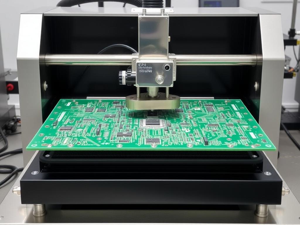
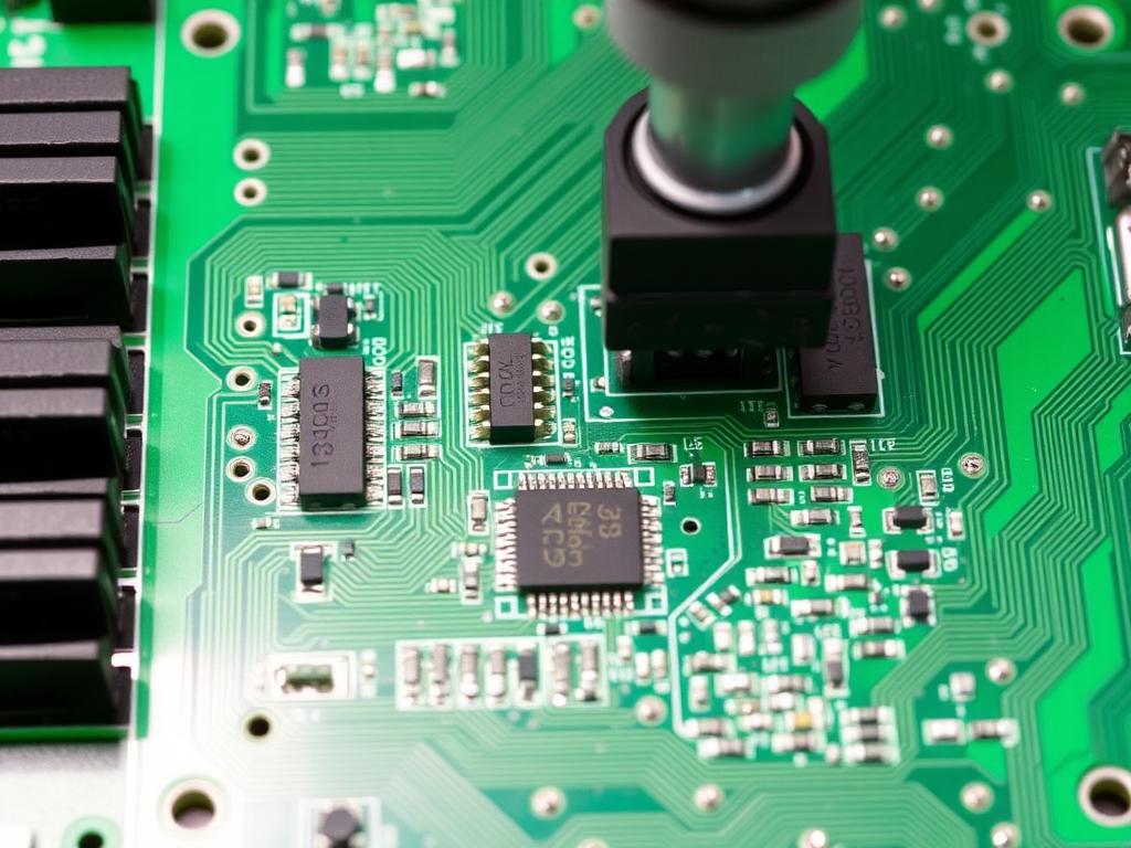
3. How Does the PCBルーター Machine Work and Where is it Best Used?
の PCBルーター has become a workhorse in PCB パネルの取り外し. From my experience, I’ve seen it bridge the gap between simple V-scoring and the precision of レーザーデパネル. So, how does it work? A PCBルーティング machine uses a high-speed rotating milling bit, guided by a computer-controlled process, to accurately separate プリント基板 から 大きなパネル。 基板 panel is often held in place by a 備品, ensuring the ルーティング process is precise and consistent. This tool is used to create clean and accurate edges on the 回路基板.
A key advantage of a ルーター is its versatility. Unlike パンチ depaneling, which requires a special fixture for each design, a ルーター can handle a variety of shapes and sizes. The machine follows a programmed path, enabling it to cut curves and sharp corners with ease. This is particularly important when dealing with complex 基板 designs that have intricate outlines. For rigid flex pcbs、 ルーター machine is also the best choice.
We’ve supplied many of our PCBルーターマシン to major electronics manufacturers like TP-LINK, Canon, BYD, Flex, TCL, Xiaomi, Lenovo, OPPO, HONOR, and Foxconn. They have found it to be reliable for a wide range of PCB パネルの取り外し needs, whether it’s 個別のPCB or multiple individual circuits. One of the core advantages of routing is that it minimizes stress on components during the 別 process, unlike manual methods that can introduce significant 機械的ストレス.
4. What are the Advantages and Disadvantages of Mechanical PCB Routing?
As I’ve witnessed over the years, mechanical PCBルーティング offers a solid balance of versatility and efficiency, but it isn’t without its limitations. The advantage of speed and flexibility that ルーティング provides makes it a great fit for many production environments, but it’s important to understand the potential drawbacks. Here’s what I’ve learned:
利点:
- 汎用性: As mentioned before, ルーティング can handle various shapes, sizes, and materials. This makes it ideal for プリント基板 with complex designs, curves and sharp corners, as well as boards with multiple individual circuits に 大きなパネル.
- 機械的ストレスの軽減: Unlike hand breaking, and v-cut methods, ルーティング minimizes the part induced stress の上 プリント基板, reducing the risk of damage to sensitive components, particularly those especially those close に edge of the board.
- 正確さ: の computer controlled process の ルーティング ensures accuracy in cutting, resulting in cleaner edges. This is critical for subsequent assembly processes.
- Cost Effective: While the initial investment might be higher than simpler methods, the long-term operational costs of ルーティング are very reasonable and suitable for medium to large volumes.
- Suitable for Flex Circuit: Unlike mechanical dies or パンチ method, ルーター machine is suitable for various type of material including フレックス material.
Disadvantages:
- Tool Wear: The milling bits used for ルーティング wear out over time and require replacement. However, this can be mitigated by choosing suitable quality milling cutters like our Milling Cutter.
- Cutting Oils: The use of cutting oils can add additional steps to the process.
- Dust and Debris: ルーティング generates dust and debris, requiring proper ventilation and cleaning systems to maintain a clean working environment.
- Slower Than Punching: For very large volumes of identical プリント基板, パンチ depaneling might be a slightly faster method.
We have developed several routing machines, from the GAM 380AT PCB 底部パネル剥離機, to the GAM 330AT インライン自動 PCB ルーターマシン. These are designed to mitigate the drawbacks, focusing on efficiency and cleanliness. Over the past years, I’ve seen the technology behind these machines become more advanced, allowing the process to be much more precise and cost-effective.
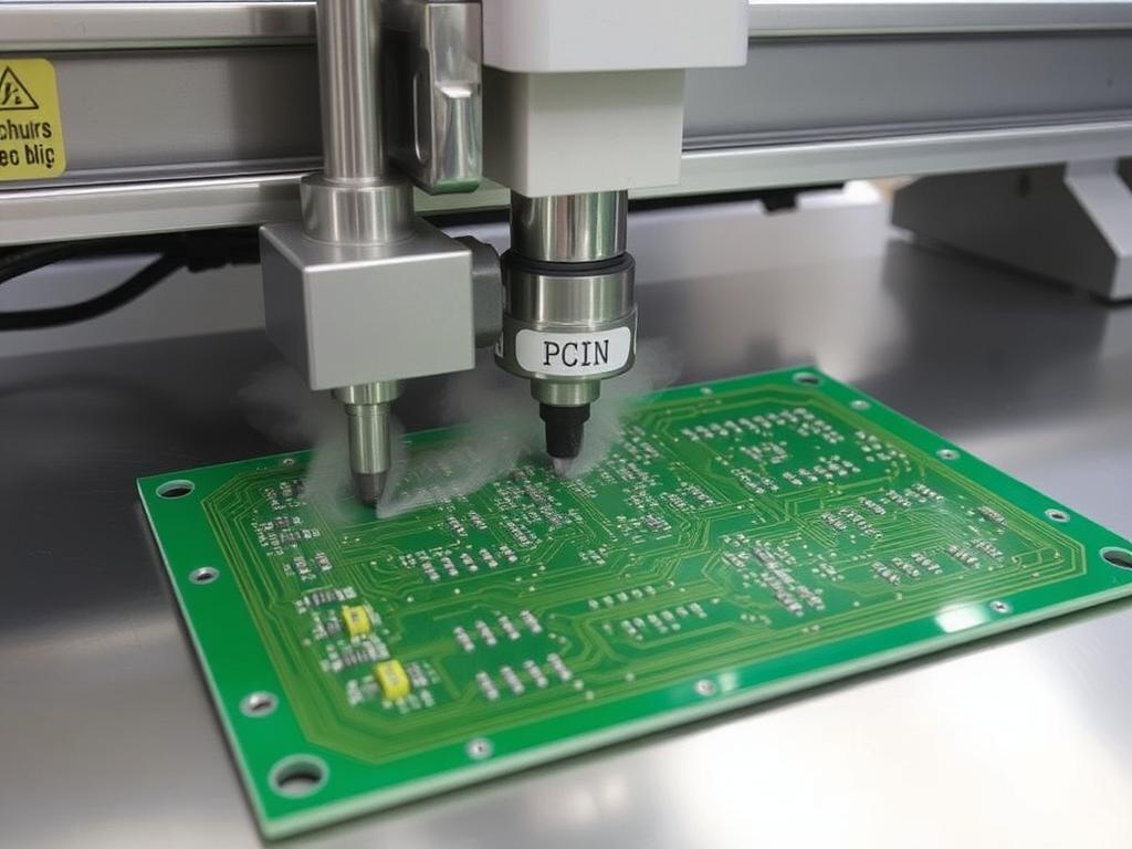
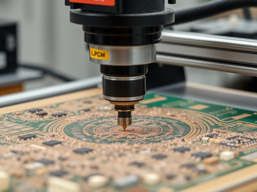
5. How Does レーザーデパネリング Compare to Traditional Methods and is it Better?
レーザーデパネル has emerged as a game-changer in the PCB パネルの取り外し world. As someone who has seen the industry shift manual to laser, I can say it offers unprecedented precision, speed, and flexibility, but it comes at a cost. Let’s discuss how レーザーデパネル compares to more traditional methods.
Traditional methods like manual snapping, or Vカット methods often rely on creating a weaker line that can be easily broken. While cost effective, they often introduce unwanted stress into the board. レーザーデパネル, on the other hand, is a non-contact process. Instead of a mechanical force, a レーザールーティング beam is used to precisely ablate the material along the separation line. This reduces the part induced stress and eliminates the risk of physical damage from tooling, making it perfect for very sensitive プリント基板 または フレックス 基質。
レーザーデパネリングの利点:
- 高精度: レーザーデパネル provides a very high degree of accuracy, with a cut kerf width の less than 20 microns.
- 最小限のストレス: The non-contact レーザー切断 process significantly reduces 機械的ストレス, making it ideal for delicate プリント基板 そして フレックス 回路。
- 柔軟性: レーザーデパネル is capable of cutting complex shapes, カーブと鋭角 with extreme accuracy.
- Clean Cut: It produces very clean and smooth edges with no burrs or debris, reducing the risk of dust and contamination.
- Suitable for Small PCBs: When dealing with 小型PCB used in complex electronic devices, レーザールーティング offers great precision where other methods might fail.
Disadvantages of Laser Depaneling:
- Higher Initial Cost: The equipment for レーザーデパネル is significantly more expensive compared to traditional mechanical methods.
- Noticeable Heat Effect: Although minimal, there is some heat generated during レーザーデパネル, which can have an effect on certain materials.
- Slower Than Some Methods: While fast, レーザーデパネル can be slower than パンチ depaneling for very high volumes of identical boards.
Our experience shows that while the initial investment in レーザーデパネル is higher, the benefits of reduced stress, increased accuracy, and overall quality often outweigh the cost, especially for high-value プリント基板 複雑で フレックス回路 designs. We’ve seen a growing adoption of レーザーデパネル in the industry. Our DirectLaser H5 PCB-FPC レーザー切断機 そして DirectLaser H3 レーザーオンラインマシン are testaments to the effectiveness and advancement of the technology.
6. When is パンチ Depaneling the Right Choice for PCB(プリント基板)?
パンチ depaneling, while not as versatile as ルーター または レーザーデパネル, still holds its ground as a valuable method in specific scenarios. In my two decades in this industry, I’ve seen its strength in high-volume production of identical プリント基板 where the design is relatively simple and well-defined.
のプロセス パンチ depaneling involves using a mechanical die, customized to the specific shape of the individual circuits. This die is pressed onto the 基板 panel, and the boards are broken out of the panel. It is a fast and relatively efficient method for high production quantities.
Advantages of Punch Depaneling:
- 高速: For large volumes of identical プリント基板, パンチ depaneling can be significantly faster than routing or laser. The advantage of speed makes it an attractive option for high-volume manufacturers.
- Lower Operational Cost: Once the tooling is created, the operational cost per board is lower.
- Consistent Results: The process is very repeatable, ensuring consistent results across all the boards on the panel.
Disadvantages of Punch Depaneling:
- High Tooling Cost: The initial tooling cost is high, as you need to manufacture a custom die for each 基板 design. This can be prohibitive for smaller production runs.
- Lack of Flexibility: Unlike routing, punch depaneling is not suitable for complex shapes, curves or sharp corners. Each 基板 design requires a different die.
- Mechanical Stress: It can also introduce more 機械的ストレス on the components compared to ルーター または レーザーデパネル, which can damage sensitive parts, particularly if they are near the separation line.
- Not suitable for flex: パンチ depaneling is not suitable for フレックス material.
In our experience, we’ve seen パンチ depaneling favored by manufacturers producing large quantities of identical, simpler boards, where tooling cost is amortized over a high production volume. For instance, in the production of basic electronics like consumer gadgets. However, its inflexibility and limitations make it less suitable for complex 回路基板 and prototypes, and it definitely doesn’t come anywhere near the precision of レーザーデパネル。 私たちの ZM10T & 15T PCB & FPC パンチングカッティングマシン are examples of our commitment to this method, offering robust and reliable performance.
7. What is V-Cut Depaneling and How Does it Impact Manufacturing?
V-cut depaneling is another method I’ve seen frequently used in the industry. It’s a process that involves creating a V-shaped groove (vスコア) on the top and bottom surfaces of the 基板 panel along the intended separation line, allowing the boards to be snapped apart relatively easily. In essence, it pre-weakens the material so that the 個別のPCB can be broken out of the panel with minimal force.
で Vカット depaneling, the panel are scored using a specialized tool. The depth of the vスコア needs to be carefully controlled, ensuring that it’s deep enough to facilitate easy separation but not so deep that it weakens the 基板 too much. The method relies on manual or machine-assisted separation after the vスコア is complete.
Advantages of V-Cut Depaneling:
- コスト効率が高い: It’s a relatively inexpensive method, particularly for high volumes of simple designs.
- Fast and Efficient: のプロセス panel are scored is quick and efficient, making it suitable for large scale production.
- Simple Process: It doesn’t require complex machinery or specialized skills.
Disadvantages of V-Cut Depaneling:
- Mechanical Stress: The snapping process can induce 機械的ストレス, particularly on 半田 joints and components that are close to the separation line. This can lead to board damage and failures.
- Limited Design Flexibility: It is not suitable for プリント基板 with complex shapes, カーブと鋭角, or those that require a precise separation path. It works best for straight line separation.
- Less Precise than other methods: The breaking step can create an uneven and rough board edges.
- Not Suitable for Flexible Materials: When it comes to flexible materials such as フレックス, v-scoring isn’t the best solution. The フレックス material can get damaged when broken out of the panel, and it doesn’t guarantee a clean 別 ライン。
We understand the trade-offs involved with Vカット depaneling, and our range of V溝デパネル 機械、例えば ZM30-ASV 全自動鋸型V溝PCBデパネル そして ZM30-P PCBギロチンセパレーター, aim to maximize the benefits of this method while mitigating its inherent limitations. While this method is commonly used in the industry, it’s important to carefully consider its drawbacks, particularly when dealing with higher value or complex 回路基板.
8. Why is Precision and Minimal 機械的ストレス so Crucial in Circuit Board パネル取り外し?
Precision and minimal 機械的ストレス are non-negotiable requirements in modern 回路基板 depaneling. Over the years, I’ve seen firsthand the repercussions of poor separation techniques. The impact on the quality and reliability of the final product is enormous, which is why we have strived to develop solutions that minimize both.
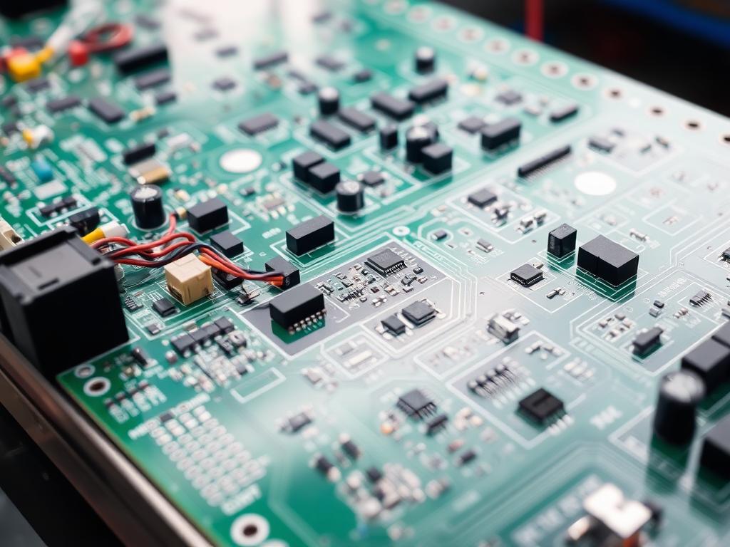
Why is this so crucial? First, 回路基板 are packed with delicate components and intricate traces. These components, especially those using 表面実装技術, are extremely sensitive to physical forces. Applying too much 機械的ストレス その間 パネル除去プロセス can cause cracks in the はんだ接合部, component damage, or even delamination of the board itself. These damages are not always immediately apparent but can lead to premature failure in the field.
Second, modern electronics have become incredibly complex, often involving multiple layers and intricate 回路 layouts. Any deviations from the intended separation path can sever traces or other delicate features, rendering the board unusable. This is especially true when dealing with 小型PCB and tight spaces. This is where precise レーザー切断 shines.
Finally, quality and reliability are crucial factors in the competitiveness of products, especially in high-stakes sectors like aerospace, medical devices, and automotive. The cost of failure is far higher than the cost of investment in good equipment.
Achieving precision and minimal stress requires using the right パネル分割システム, whether that’s a carefully programmed router cutting machine or a レーザールーティング system. Proper 備品, precise alignment, and controlled forces are also crucial to maintaining the integrity of every board. For us, it’s not just about 個人を分離する boards, it’s about ensuring that each board is ready to perform its intended function reliably for a long time. Our commitment to precision is evident in every one of our products, from our automated solutions to our precision cutting tools.
9. How Can Automation Improve the Depaneling Process そして Increase Production Line Speed?
Automation has dramatically transformed the PCB パネルの取り外し landscape, and for the better. In the past, much of the process was done manually, which was slow, inconsistent, and prone to errors. In today’s 製造工程 world, automation plays a key role in ensuring a high level of production line output and reducing waste.
Automation brings many advantages to the パネル除去プロセス. First and foremost, it increases speed. Automated machines can process many boards per hour compared to manual operations. The increase in production line speed directly translates into reduced production times and lower operational costs. Also, automation ensures consistency, a critical factor in high volume production, especially when working with 回路基板 that require high precision.
Moreover, automated systems reduce the need for manual labor, minimizing the risk of human error and workplace injuries. When coupled with vision systems and advanced software, automated depaneling machines can detect and rectify any misalignment or issues immediately, guaranteeing that each board is separated correctly. This is something we, at pcbdepaneling.com, focus on a lot.
We have developed a variety of automated solutions, including Automatic Plate Palletizing Machines そして Automatic Sorting and Palletizing Machines, designed to work seamlessly within your systems that increase production line. These machines integrate smoothly with existing production lines and reduce the need for manual intervention. The use of automation not only improves the パネル除去プロセス but also increases the efficiency and profitability of the entire production line. Our experience shows that investing in automated systems is a step towards increased efficiency, reduced waste, and improved product quality.
10. How Do I Choose the Best デパネルシステム for My PCB(プリント基板)?
正しい選択 デパネルシステム あなたの プリント基板 can make all the difference in the efficiency, quality, and cost-effectiveness of your production. The best system is dependent on several factors, and there’s no “one-size-fits-all” solution, it’s very important to assess all relevant factors. Here are some factors that should play a role in your decision.
- 生産量: If you are processing a high volume of identical boards, a パンチ depaneling system might be suitable, if design constraints allow for it. If you produce small quantities of boards with complex shapes and カーブと鋭角, then a ルーター または レーザーデパネル system might be a better choice.
- PCB Design Complexity: Complex designs with tight components require a precise and low-stress method, making レーザーデパネル or precision ルーティング your preferred option. Simple designs with straight separation lines are fine with a v-cut or パンチ method.
- Material Sensitivity: If you have sensitive components that are close to the separation line, レーザーデパネル should be considered due to its minimal 機械的ストレス. フレックス materials will also need a more careful approach, and ルーター または レーザーデパネル are the best choice in that case.
- 予算: The initial cost of レーザーデパネル is high, so if you are operating within a limited budget, then a ルーター machine would be a better choice, as it provides an excellent balance between accuracy and cost.
- Required Line Speed: If your production line needs to be really fast, a パンチ method is still valid for certain types of circuit boards, but is not as flexible as ルーター または レーザ システム。
- Long Term Costs: Consider not only the initial cost but also the operational costs, including tool replacement, energy consumption, and waste disposal. While レーザーデパネル has a higher initial cost, it might provide long term cost benefits due to it’s precision, low stress, and clean cuts.
For a lot of our clients, the role in the manufacturing process of depaneling machines is critical. When choosing your パネル分割システム, you should always look for a reliable supplier that can provide not only top quality machines, but also technical support and parts when you need them. We have the necessary experience to help you choose the right system.
よくある質問
What is the difference between PCB depaneling and PCB singulation?
There is virtually no difference between PCB depaneling and singulation. Both terms refer to the 分離のプロセス 個人 プリント基板 より大きなパネルから。
Can I depanel PCBs with components on them?
はい、 PCB パネルの取り外し is usually done after the components are mounted, but it should always be done with appropriate care to avoid damage to the components or はんだ接合部.
What method should I use for my flex PCBs?
のために flex pcb depaneling plays a pivotal role. Given the sensitive nature of flexible materials, the best options for フレックス circuits are either ルーター または レーザーデパネル. Both of these methods provide the necessary precision and low stress needed to prevent material damage.
Is Laser depaneling really worth the high cost?
It really depends on your specific situation. While the initial investment is higher, the benefits of precision, minimal stress, and the ability to handle complex designs may offset the higher cost, especially for high-value boards.
What kind of maintenance do PCB depaneling machines require?
The maintenance requirements vary. A ルーター machine will require regular bit replacement and cleaning. レーザーデパネル machines will require cleaning of the レーザー切断 head and optical components. All machines will require regular maintenance, which can be done by qualified technicians.
重要なポイント
- PCB パネルの取り外し 個人を分離するプロセスである プリント基板 from a larger panel, essential in PCBアセンブリ.
- Several methods exist, including manual separation, Vカット, パンチ, ルーター、 そして レーザーデパネル.
- ルーター machines are versatile, suitable for complex shapes, and minimize part induced stress, but they require regular maintenance.
- レーザーデパネル provides high precision and minimal stress, ideal for small, delicate プリント基板 そして フレックス materials, though with a higher initial investment.
- パンチ depaneling is ideal for high-volume production of identical, simple boards, but is inflexible and has high tooling costs.
- V-cut depaneling is cost effective for straight lines, but may introduce 機械的ストレス に はんだ接合部.
- Automation enhances speed, consistency, and reduces errors in the パネル除去プロセス.
- Choosing the correct デパネルシステム depends on your production volume, design complexity, budget, and desired quality.
As a veteran in the industry, I’ve dedicated my career to understanding and improving the パネル除去プロセス. My goal is to provide solutions that are both innovative and practical, helping you achieve your manufacturing goals. If you’re looking to improve your own process, we invite you to explore our range of products on our website, or contact us for more detailed assistance. You can learn more about our PCBルーターマシン, explore our V溝デパネル, check out our PCB/FPCパンチングマシン, discover our 自動装置, find the perfect アクセサリー, and explore our SMT全ライン設備 as well as PCB レーザーによるパネル剥離 ソリューション。