![]()

Automated PCB depaneling process
Cutting Edge: A Comprehensive Guide to PCB Depaneling Methods, Focusing on Laser Precision
Hey there, fellow PCB enthusiast! With 20 years in the trenches of PCB manufacturing, I’ve seen it all. This article isn’t just another technical piece; it’s a deep dive into the world of PCB depaneling, focusing particularly on the magic of laser technology. We’ll explore various methods, weigh the pros and cons, and I’ll share insights that come from years of hands-on experience. Whether you’re an electronics tech company, a massive production factory, or even an independent PCB tinkerer, understanding these processes is crucial for efficient, high-quality production. We, as a leading manufacturer, serve giants like TP-LINK, Canon, BYD, and many more, so you know you’re getting the real deal.
1. What exactly is PCB Depaneling and Why is it Important?
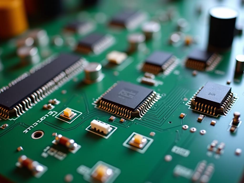
PCB depaneling is the process of separating individual pcbs from a larger panel after the circuit boards are assembled. Think of it like cutting cookies from a sheet of dough – instead of cookies, we’re dealing with delicate electronic components on a printed circuit board. This 分離プロセス は、 製造工程, ensuring each individual pcb is ready for its intended application. Without proper depaneling, you risk damaging the delicate 半田 joints, causing 機械的ストレス and compromising the functionality of the 基板. From my two decades in the industry, I’ve seen firsthand how critical a precise, careful パネル除去プロセス is to PCB製造.
Imagine producing hundreds of circuit boards on a single panel only to have them ruined during the separation. The consequences of improper depaneling are wasted material, time, and increased costs. Efficient PCB パネルの取り外し not only ensures quality control, it also has a significant impact on the ワークフロー, by streamlining the process and contributing to the 費用対効果 of the entire 製造工程. It also allows for better handling and integration into final products. We understand these challenges intimately, which is why we focus on developing パネル取り外し機 that offer both precision and speed.
2. What are the different methods of PCB depaneling?
Over the years, many PCB パネルの取り外し方法 have been developed, each with their own pros and cons. These methods range from manual, mechanical techniques to highly automated, advanced processes.
- Manual Depaneling: This involves scoring the 基板 and breaking it apart by hand or with a simple tool. While low-cost, it’s slow and prone to errors, not a good fit for the high-volume or sensitive プリント基板 in modern electronics.
- V-Groove Depaneling: これ method uses a scoring saw to cut grooves on the top and bottom of the 基板, which weakens the material and allows the boards to be separated. It’s faster than manual separation, but can still create stress on the components if not done right. Our V溝デパネル solutions are designed to minimize that stress.
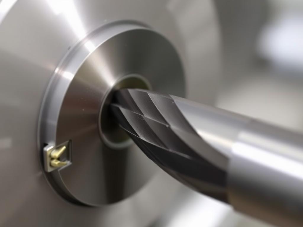
- ルーティング: PCBルーティング employs a ルーター または milling machine カットする 基板 along predefine contours. Milling machines provide good accuracy, but they can be slow and produce dust that needs to be managed and the use of a ルーター can cause some problems like heat build-up in certain materials.
- パンチング: PCB/FPCパンチングマシン utilizes a die to separate the pcbs. This works well for pcbs with simple outlines, however more complicated shapes will not allow this type of 切断工程.
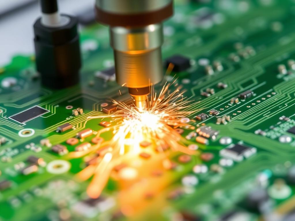
- レーザーデパネル: The process uses a レーザービーム に ablate の 基板 material along a designated path, which precisely cuts or 個別化 the pcbs. This is the most precise and versatile 切断方法, offering excellent control, but requires a higher initial investment.
Each of these methods has their place, but as we delve deeper, you will see why レーザーデパネル stands out, particularly when PCBの切断 with high precision and efficiency are required.
3. Why is Laser Depaneling gaining popularity?
レーザーデパネル is rapidly becoming the preferred デパネル工法 in the electronics industry. Why? Because it offers 大きな利点 over traditional pcb depaneling methods. First, it’s incredibly precise. A 集中レーザービーム can ablate even the most delicate 基板 material with amazing accuracy. This is crucial when dealing with increasingly smaller and densely packed components.
Second, レーザーデパネル は without physical contact process. Unlike mechanical separation, レーザー切断 introduces minimal mechanical or thermal stress に 基板. This reduces the risk of damaging sensitive 表面実装 components and maintains the integrity of the 半田 joints. This is a significant advantage for manufacturers focused on quality and reliability. As electronics become more sophisticated and fragile, the use of lasers will only increase. For example, we see how our DirectLaser H5 PCB-FPC レーザー切断機 consistently provides a superior finish over traditional methods. The future of depaneling is here.
4. How does Laser Cutting achieve high precision in PCB depaneling?
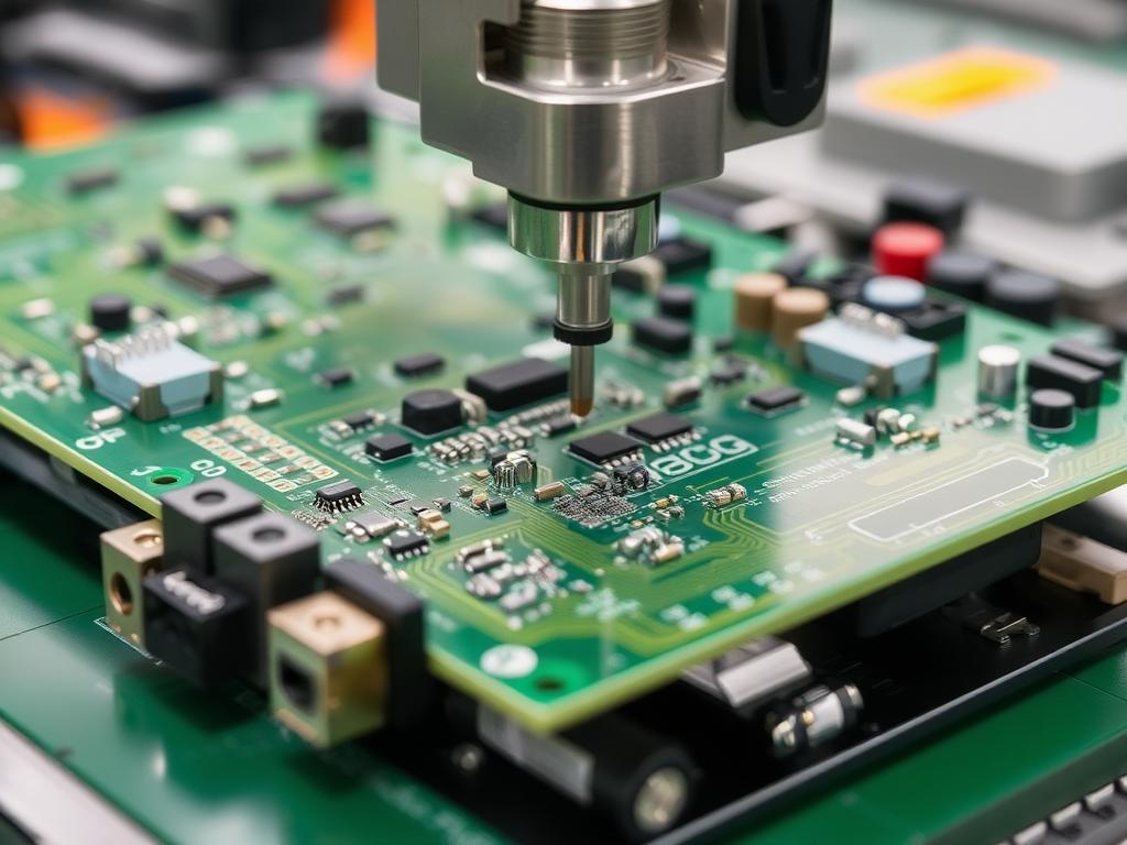
The secret to the precision of レーザー切断 lies in its ability to control the レーザービーム. Unlike a mechanical blade or a router, which can introduce physical pressure and vibrations, a レーザービーム is non-contact. The レーザーシステム precisely remove material layer by layer at a specific 切断速度, using intense energy to ablate の 基板 along a pre-programmed 輪郭.
の レーザー加工 allows us to achieve incredibly small cutting channel widths, often measured in µm, ensuring minimal material removal and maximum accuracy. This is especially important when dealing with densely populated プリント基板 where components are placed very close to the 輪郭. This level of precision is difficult to achieve with other パネル分割方法. The control and precision offered by レーザーデパネル means that pcb designers can push the limits of design and functionality, knowing that the 分離プロセス will not compromise the final product.
5. What are the key benefits of using a Laser Depaneling System?
投資する レーザーデパネルシステム might seem like a big jump, but the return on investment comes in many forms. Let’s look at some key benefits:
- 優れた精度: As I’ve stressed, the precision of laser cutting is unmatched. This means fewer errors, reduced rework, and better quality overall.
- ストレスの軽減: Laser depaneling doesn’t apply 機械的ストレス on the components or 回路基板, greatly reducing the chances of damage, which is especially critical when dealing with delicate surface mount devices.
- 柔軟性: レーザーシステム can cut complex shapes and contours with ease and are suitable for various type of pcb materials and material thicknesses. You are not limited to straight cuts or simple designs.
- 清潔さ: The laser cutting プロセス creates very little dust and debris compared to routing, meaning your workspace and your products stay cleaner.
- オートメーション: レーザーデパネルシステム are easily integrated into オートメーション solutions, streamlining the entire 製造工程 and increasing efficiency. A SMT インラインデパネリングマシンソリューション 劇的に改善できる スループット.
- 汎用性: レーザーシステム can be used for other tasks like marking, and even engraving on プリント基板. This further enhances its value.
From my perspective, if you are looking for the highest quality, most flexible, and most efficient depaneling solution, レーザーデパネル offers significant advantages and should be high on your list.
6. What Design rules should you consider for Laser depaneling?
Like any manufacturing process, laser depaneling has its own 設計ルール. These guidelines ensure that the separation process is successful and the integrity of the final product is maintained. Here are a few crucial aspects to consider in the design process:
- Clearance: Ensure there’s enough space between the cutting channel and the nearest components. This prevents the レーザービーム from accidentally damaging components during the 切断工程.
- Fiducials: Fiducials are markers placed on the 基板 to guide the laser system 中に 切断工程. These need to be placed accurately to ensure precise ルーティング そして 切断.
- パネル化: Panelization is the way multiple プリント基板 are arranged on a single panel. This must be planned carefully to ensure efficient ルーティング and easy 分離プロセス と レーザ.
- Material Thickness: Be sure to consider the material thickness when working with a レーザ. Each material, and their unique characteristics, respond to laser differently, and require different settings. Ensure that the レーザーシステム are adjusted to suit the materials and thicknesses.
- Component Height: When placing components, it’s important to consider the height of the components. Taller components need to be clear of the intended cutting line of the レーザ.
By following these 設計ルール, you can ensure that the laser depaneling process runs smoothly. This proactive approach leads to fewer problems during PCB製造. Our team can help you navigate these design rules and ensure optimal results.
7. Can Laser depaneling enhance throughput in PCB manufacturing?
絶対に。 レーザーデパネル not only provides superior precision and reduced stress but it can also significantly increase スループット で PCB製造. How? Primarily through automation.
モダンな レーザーシステム can be easily integrated into fully オートメーション 行。 完全自動 systems significantly reduce the need for human intervention, which reduces human error and speeds up the whole ワークフロー. With a 全自動 レーザー切断機, boards are moved, cut, and collected efficiently. This also results in consistent 品質管理. We see how our GAM 630V 自動仕分け・パレタイジングマシン can be integrated with レーザーシステム to create a seamless, high-スループット manufacturing solution. With high speed 切断速度 and a large working area, our レーザー加工機 can significantly reduce the time it takes to depanel a batch of プリント基板.
8. What challenges do designers face when implementing traditional pcb depaneling?
その間 traditional pcb depaneling methods are still used, they present several design challenges のために pcb designers.
- Mechanical Stress: Methods like ルーティング または V溝加工 can introduce 機械的ストレス に 基板、敏感な部品に損傷を与える可能性がある、または 半田 joints. This is particularly a concern for 小型PCB and boards with surface mount technology components are placed.
- Limited Flexibility: Traditional methods are limited in the shapes and contours they can produce. This can constrain the design freedom の 基板 and require the designer to predefine their limits.
- Dust and Debris: Methods like routing create dust and debris that need to be managed, and cause issues in the production processes and require additional cleaning steps.
- Precision Limits: これら 方法 are limited in the precision they can achieve. This is problematic when dealing with highly complex and densely populated プリント基板.
I’ve seen designers struggle with these limitations, often having to make trade-offs that impact the final product. These PCBの課題 depaneling are exactly what レーザーデパネル is designed to address and overcome.
9. How do I choose the right Depaneling machine for my PCB production needs?
正しい選択 パネル取り外し機 あなたの特定の individual requirements そして PCB製造 volume and budget. Let’s break down the factors to consider:
- Volume and Throughput: If you have a low-volume operation, a スタンドアロン 機械 might suffice. For high-volume operations, invest in an in-line, fully オートメーション solution to enhance スループット.
- 精度要件: If you are dealing with delicate or complex プリント基板、 レーザーデパネルシステム is a must-have. For less demanding applications, V溝 または ルーターマシン may be adequate.
- 予算: Initial investment costs are a factor. Laser systems tend to have a higher upfront cost, but offer better 費用対効果 over time.
- Space: Consider the available space when planning your set-up. Laser machines are more compact, and our GAM 320AL 自動 PCB ルーターマシン is an excellent example of a modular 解決。
- 材質タイプ: Not every method is suitable for every type of pcb material. It is important to research, and confirm that the correct 切断方法 is used for your material.
- Ease of Use and Maintenance: Look for パネル取り外し機 that are user-friendly and have low maintenance requirements, which will save you time and money over the long term.
We at PCB パネル分割 understand these varying needs and can help you choose the デパネルシステム that is perfectly suited to your situation.
10. What are the Automation trends in PCB depaneling?
オートメーション is the future of PCB製造、 そして パネルを外す is no exception. Here are some trends:
- インラインシステム: Integration of depaneling machines into smt assembly lines enhances スループット, reduces material handling and streamlines the whole ワークフロー.
- Robotics: The use of robotic arms to move and position panels further enhances 自動化ソリューション and precision. Our ルーターマシン&ロボットアーム&自動プレートセッティングマシン showcase how these can be seamlessly combined.
- AIと機械学習: The use of AI for real-time adjustments to laser settings and path based on variations in the board material is emerging.
- データ統合: Automated systems provide valuable data for quality control and process optimization. レーザーシステム allow for very precise analysis and feedback.
- モジュラー設計: The use of modular designed units that can easily be upgraded or replaced. This allows PCB製造 facilities to add new capabilities without large capital expenses.
The goal is to create a completely automated, hands-free manufacturing process, which will reduce errors, improve スループット and maintain 品質管理。 これら オートメーション trends are transforming PCB製造, and we are at the forefront of this revolution.
FAQs:
What is the typical lifespan of a laser used in a depaneling machine?
The lifespan of a laser depends on the type of laser and usage. Generally, 紫外線レーザー used in our レーザーシステム have a very long operational life, and need to be replaced less frequently, however, regular maintenance will ensure peak performance.
Can Laser depaneling cut through thicker pcbs?
Yes, with the correct settings and power, レーザーデパネル is able to cut through various material thicknesses. However, it is important to adjust the settings according to the requirements of the material.
Is it possible to perform laser depaneling on assembled printed circuit boards?
はい、 レーザーデパネル is perfect for 組み立てられたプリント基板 because of its non-contact nature. It doesn’t apply any mechanical or thermal stress, which is critical to protect the components.
Does Laser depaneling require special environment or special exhaust system? レーザーシステム do generate some fumes and require an exhaust system, however, this is usually integrated into the laser machine. We recommend a clean space, and that the デパネルシステム is well-maintained.
How difficult is it to integrate Laser Depaneling into existing SMT lines?
We design our レーザーシステム with easy integration in mind. Modern systems often come with communication protocols that enable easy integration to smt lines. With our help, the integration can be done relatively quickly and without any problems.
まとめ:
- PCB パネルの取り外し is a critical process that separates individual pcbs from a larger panel.
- There are many methods for PCB パネルの取り外し方法, ranging from manual to highly automated processes like レーザーデパネル.
- レーザーデパネル offers superior precision, reduced stress, and greater flexibility compared to traditional pcb 方法。
- Design rules, including clearance, fiducial, パネル化、 そして material thicknesses, must be carefully considered when working with レーザー切断.
- オートメーション is transforming the PCB製造 sector and レーザーデパネルシステム are an essential part of this.
- 正しい選択 パネル取り外し機 depends on your production volume, precision requirements, and budget, depending on the specific requirements.
In my 20 years, I’ve seen the 基板 industry evolve dramatically. Laser depaneling is not just the current trend, it’s an advanced and コスト効率が良い solution that continues to evolve. If you’re looking to enhance your PCB製造 with the most precise and efficient method available, レーザーデパネル is the way to go. Let’s talk about how we can 合理化 あなたの production processes. Contact us today to learn more.