![]()

Advanced PCB depaneling techniques
From Manual to Laser: Revolutionizing PCB Depaneling for Peak Efficiency
For two decades, I’ve been immersed in the world of printed circuit boards (基板s), witnessing firsthand the evolution of their パネル除去プロセス. From the early days of painstaking manual separation to the cutting-edge precision of レーザ technology, it’s been a remarkable journey. If you’re involved in プリント基板 manufacturing, especially high-volume production, the efficiency and accuracy of your PCB パネルの取り外し methods are critical. This article delves into the transformative shift from traditional, often stressful, techniques to the streamlined power of レーザーデパネル, and why embracing these advancements is crucial for today’s competitive landscape. Understanding these PCB パネルの取り外し方法 is essential for optimizing your production line, and this is why this article is a must-read for anyone in the electronics industry.
記事の概要: PCB デパネルの世界をナビゲート
Here’s a roadmap of what we’ll explore to help you understand the best デパネル工法 for your needs:
- What are the Common PCB Depaneling Methods and Their Limitations?
- なぜ レーザーデパネリング Gaining Popularity as the Preferred プリント基板 Separation Technique?
- How Does レーザ Technology Ensure Precision in the PCB パネル分割 Process?
- いつ PCBルーター Machine the Ideal Choice for プリント基板 Separation?
- How Significantly Does レーザーデパネリング Improve Production スループット?
- What Role Does Effective PCB Panelization Play in Optimizing Depaneling?
- は パンチ Methods Still Relevant in Modern PCB パネル分割?
- How Does Proper PCB Panelization Influence the Success of Depaneling?
- What Key Considerations Ensure 品質保証 in Your Depaneling Process?
- How Do You Choose the Right Method to Depanel and Achieve Efficient Depaneling?
- What Factors Should You Consider When 適切なパネル分割方法の選択?
Decoding Depaneling Methods and Their Drawbacks
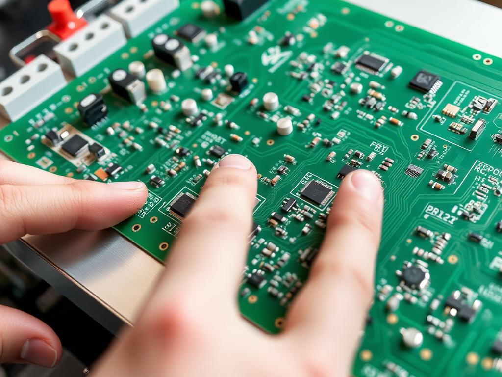
Over the years, I’ve seen various デパネル工法s come and go. In the beginning, it was often 手作業によるパネルの取り外し, a slow and laborious process prone to errors and 機械的ストレス on the delicate 回路. Imagine trying to 別 個別のPCB から 大きなパネル by hand – the risk of damaging components or the PCB材料 itself was significant. Then came techniques like Vスコアリング、ここで V溝 is pre-scored on the 基板, allowing for a controlled break along the line. While faster than manual methods, Vスコアリング still introduces 機械的ストレス and can leave rough edges. Using a パンチ press to force individual printed circuit boards out of the pcb panel was another approach, suitable for simpler designs but often leading to deformation and limitations on PCB設計. Even using sharp blades on one part and supports on another part could introduce unwanted stress and inconsistencies. These traditional PCB パネルの取り外し方法, while sometimes 費用対効果が高い for low-volume production, often struggle to meet the demands of high スループット and stringent quality requirements in modern PCB製造.
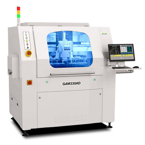
The Rise of Laser Depaneling: Precision and Efficiency Redefined
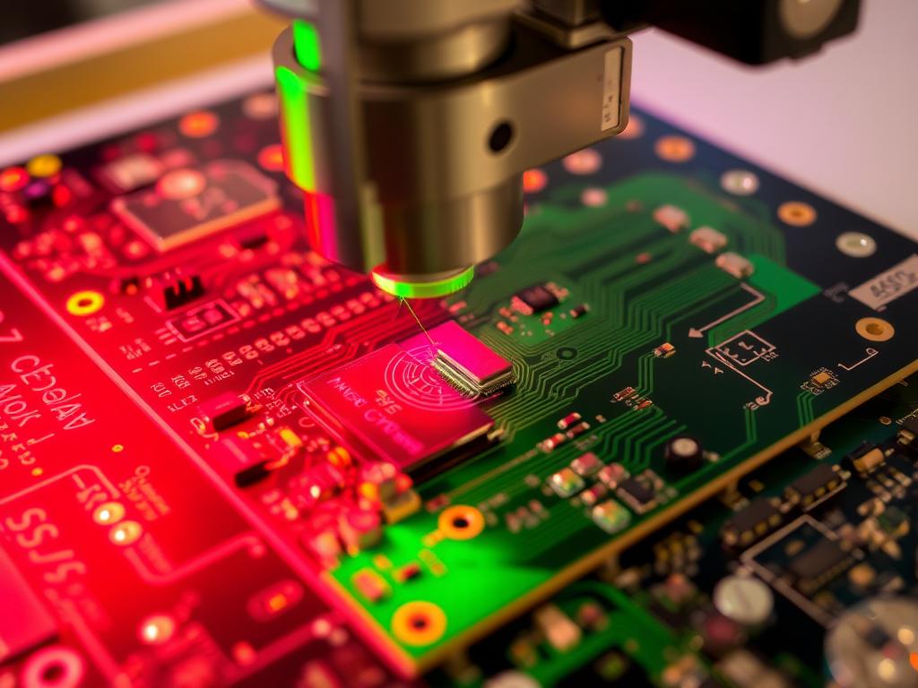
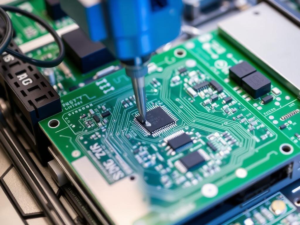
の出現 レーザーデパネル has truly revolutionized the field. Instead of physical force, a highly 集中レーザービーム 正確にカット 基板, leaving clean, smooth edges and eliminating almost all 機械的ストレス. From my perspective, witnessing this transition has been incredible. The ability of レーザ technology to accurately follow complex contours and 別 intricate board designs is unmatched. The レーザー切断 process is non-contact, meaning there’s no direct force applied to the 基板, drastically reducing the risk of damage. This is especially crucial for sensitive components and thin PCBの厚さ. Whether it’s a rigid or flex circuit substrate, レーザーデパネル offers a level of 精度と品質 that traditional methods simply cannot match. The fine 切り口幅 achievable with レーザーシステム also allows for denser パネル化, maximizing material utilization from a 大きなパネル. This leap in technology addresses many limitations of older techniques, making レーザ a top contender for efficient and high-quality パネルを外す.
Laser Precision: A Closer Look at the Cutting Edge
The magic of レーザーデパネル lies in its pinpoint accuracy. The finely 集中レーザービーム, often a 紫外線レーザー for its ability to cut through various PCB材料s cleanly, ablates the material along the desired path. Think of it like a microscopic scalpel, guided by precise software controls. This 切断工程 is incredibly accurate, ensuring that the individual printed circuit boards are 別d exactly as designed. The レーザー出力、スピード、そして 焦点スポットサイズ can be adjusted based on the PCBの厚さ and material, allowing for optimization for different type of pcb. This level of control minimizes debris and heat-affected zones, crucial for maintaining the integrity of the 回路. Having worked with various レーザーシステム, I can attest to their consistent performance and ability to handle even the most complex PCBに沿って intricate outlines. The use of 紫外線の波長が短い further enhances the precision and reduces thermal effects, making it ideal for delicate pcb technology.
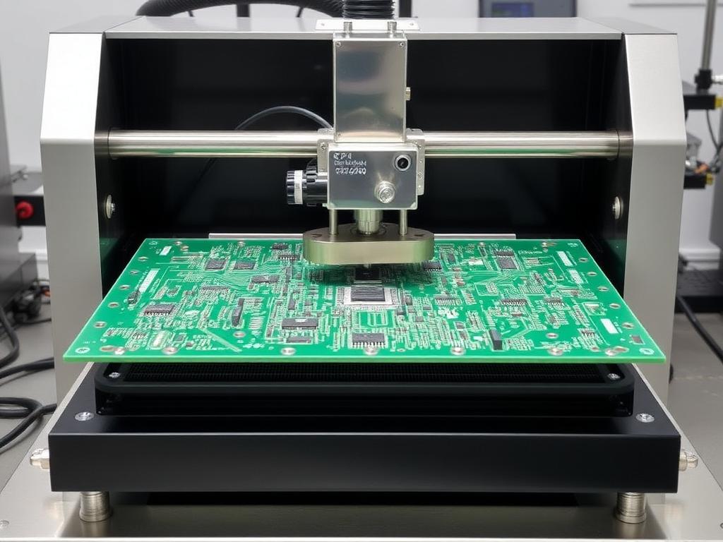
When Does a PCB Router Machine Still Shine?
の進歩にもかかわらず レーザーデパネル, PCBルーター machines remain a valuable tool in certain situations. A ルーター utilizes a spinning ルータービット to physically cut through the 基板. While it does introduce some 機械的ストレス, modern PCBルーターマシンs offer high speed and can be 費用対効果が高い for specific applications, particularly for thicker boards or when dealing with complex タブ removal. In my experience, ルーター machines excel in situations where the PCB設計 has readily accessible routing paths. They are also a well-established technology with a lower initial capital investment に比べ レーザーシステム. However, it’s important to consider the wear and tear on the ルータービット, the potential for dust generation, and the limitations in cutting intricate internal contours compared to レーザ methods. We offer a range of PCBルーターマシンs designed for efficient and reliable performance.
Boosting Production Throughput with Laser Technology
One of the most significant advantages of レーザーデパネル is its impact on production スループット. The speed and automation capabilities of レーザーシステム dramatically reduce cycle times compared to manual or even ルーター-based methods. A レーザ can quickly and accurately cut through 基板 material, and integrated automation features allow for continuous processing of pcb panels. Imagine the difference between manually snapping boards apart versus a レーザ system seamlessly 個人を分離する boards with high speed and accuracy. This increased スループット translates directly into higher production volumes and reduced manufacturing costs. For large electronic product processing factories and even individual 基板 players dealing with significant volumes, レーザー技術は a clear path to enhanced efficiency. Our PCB レーザーによるパネル剥離 solutions are specifically designed to maximize your production output.
The Crucial Role of PCB Panelization in Depaneling Success
効果的 PCBパネル化 is paramount for optimizing the パネル除去プロセス、に関係なく 切断方法 使用済み。 Panelization refers to the arrangement of multiple 個別のPCB on a single manufacturing panel. Smart panelization techniques minimize material waste, improve handling efficiency during the 製造工程, and streamline the 分離プロセス。 のために レーザーデパネル, well-designed パネル化 ensures optimal spacing for the 集中レーザービーム and allows for continuous cutting without unnecessary interruptions. Similarly, for ルーター methods, proper パネル化 ensures accessibility for the ルータービット. Poor パネル化 can lead to increased stress on the 基板, difficulties in separating individual printed circuit boards, and ultimately, reduced quality assurance. Therefore, careful consideration of パネル化 は crucial step in pcb manufacturing to ensure a smooth and efficient パネル除去プロセス.
Punching Methods: A Look at Their Place in the Modern Era
その間 レーザ そして ルーター technologies dominate high-precision パネルを外す, パンチ methods still find application in certain niche areas. Using a dedicated PCB/FPC パンチングマシン, individual boards can be パネルから打ち抜かれた using custom-designed tooling. This method is generally suitable for simpler board shapes and high-volume production of the same design. However, the force involved in パンチing can introduce significant 機械的ストレス, potentially damaging sensitive components. The tooling also needs to be precisely manufactured and maintained, and changes in board design require new tooling, adding to the 費用対効果が高いness calculation. While not ideal for complex or delicate 基板s, パンチ methods can still be a viable option for specific, high-repetition applications where precision is less critical. We offer PCB/FPCパンチングマシンs for these specific needs.
How Panelization Shapes the Depaneling Outcome
The way you arrange your pcb panel has a profound impact on the ease and success of depanelization. Think of it like this: a well-organized puzzle is much easier to take apart than a jumbled mess. Effective PCBパネル化 considers the デパネル工法 that will be used. For instance, if using a レーザ, the layout should provide clear, continuous paths for the レーザービーム to follow. For ルーター methods, sufficient space needs to be provided for the 機械‘s cutting head to maneuver. The placement of タブs or breakaway points also needs careful consideration. Poor パネル化 can lead to increased 機械的ストレス その間 分離, making it harder to achieve clean breaks and potentially damaging components or the PCB材料. Investing time in optimizing your panelization techniques 鍵となる ベストプラクティス to ensure a smooth and high-quality パネル除去プロセス.
Ensuring Quality: The Cornerstone of Effective Depaneling
Quality assurance is paramount in the パネル除去プロセス. Regardless of the デパネル工法 used, the goal is to 別 の 個別のプリント基板 without introducing defects or damage. With レーザーデパネル, the precision of the 集中レーザービーム minimizes stress and creates clean edges, inherently contributing to higher quality. Regular maintenance of equipment, whether it’s a laser system または ルーターマシン, is crucial. Proper training for operators is also essential to ensure they understand the nuances of the chosen 実践方法. Careful inspection of パネルを取り外した boards is a final step to catch any potential issues. For instance, checking for micro-cracks or residual burrs can help identify areas for process improvement. By focusing on 精度と品質 throughout the 分離プロセス, you can minimize scrap and ensure the reliability of your final product.
Choosing the Right Path: Selecting Your Ideal Depaneling Method
適切なパネル分割方法の選択 is a critical decision that impacts your production efficiency, cost, and product quality. Consider the volume of your production, the complexity of your PCB設計, the materials used, and your budget. For high-volume production requiring intricate cuts and minimal stress, レーザーデパネル is often the superior choice. If you’re dealing with thicker boards or simpler designs and looking for a more established and potentially lower initial capital investment、 PCBルーターマシン might be suitable. For very high-volume, simple designs, パンチ methods could be considered. Ultimately, the best approach involves carefully evaluating your specific needs and weighing the pros and cons of each デパネル工法. We offer a comprehensive range of depaneling solutions, including laser, ルーター、 そして パンチ machines, and our experienced team can help you navigate these choices.
Factors to Ponder When Choosing Your Depaneling Solution
となると choosing the right depaneling solution, several factors come into play. Your production volume is a major consideration. High-volume environments often benefit most from the speed and automation of レーザーシステム. The complexity of your PCB設計 is another key factor. Intricate shapes and internal cutouts are handled with greater ease and precision by レーザ technology. The PCBの厚さ そして PCB材料 also influence the choice. Thicker boards might be more effectively processed by a robust ルーター、 その間 レーザ is excellent for a wide range of materials, including sensitive flex circuits. Your budget, including both the initial capital investment and ongoing operational costs (like tooling for パンチ methods or ルータービット replacement), needs careful evaluation. Finally, consider the level of 機械的ストレス that your components can tolerate. レーザーデパネル, with its non-contact approach, minimizes stress, making it ideal for sensitive electronics. By carefully weighing these factors, you can make an informed decision and select the デパネル工法 that best aligns with your specific requirements.
Conclusion: Embracing Efficiency and Precision in PCB Depaneling
The journey from manual 手破り の 基板s to the sophisticated precision of レーザーデパネル reflects significant progress in PCB製造. As a leading PCB パネルの取り外し machine manufacturer, we’ve witnessed firsthand the transformative impact of these advancements on our customers, including industry giants like TP-LINK, Canon, BYD, Flex, TCL, Xiaomi, Lenovo, OPPO, HONOR, and Foxconn. Whether you opt for the speed and versatility of a レーザ system, the established reliability of a ルーター, or a specialized パンチ solution, the key is to choose a method that optimizes your production スループット, maintains high quality assurance, and minimizes 機械的ストレス on your valuable 回路. Embracing efficient and precise パネル除去プロセスes is no longer a luxury but a necessity for staying competitive in today’s fast-paced electronics industry.
重要なポイント:
- レーザーデパネル offers unmatched precision and minimizes mechanical stress.
- PCBルーターマシン remain a viable option for certain applications, especially thicker boards.
- 効果的 PCBパネル化 is crucial for optimizing any デパネル工法.
- Careful consideration of production volume, board complexity, and budget is essential when selecting a depaneling solution.
- Prioritizing quality assurance throughout the depaneling process is paramount.
FAQs: Your Questions About PCB Depaneling Answered
What are the main advantages of using a laser for PCB depaneling? Laser depaneling offers high precision, minimal mechanical stress, clean cut edges, and the ability to process intricate board shapes efficiently.
Is laser depaneling suitable for all types of PCB materials? Yes, laser depaneling, particularly with UV lasers, can effectively process a wide range of PCB materials, including FR-4, flex circuits, and more.
How does a PCB router machine compare to laser depaneling in terms of cost? PCB router machines typically have a lower initial investment cost compared to laser systems, but factors like tooling and bit replacement should be considered in the long run.
What role does automation play in modern PCB depaneling? Automation significantly increases throughput and reduces manual handling, making the depaneling process more efficient and consistent, especially with laser and advanced router systems.
What factors should I consider when deciding between laser and router depaneling? Consider your production volume, board complexity, material types, budget, and the level of mechanical stress your components can withstand.
Ready to elevate your PCB depaneling process? Contact us today to explore the best solutions for your needs!
Explore our range of PCB Router Machines Learn more about our advanced PCB Laser Depaneling solutions Discover our efficient V-Groove Depaneling options See our durable PCB/FPC Punching Machines Explore our range of Automatic Equipment for streamlined production View our selection of high-quality Accessories