![]()

Cost comparison of PCB depaneling methods
Precision PCB Depaneling: Choosing the Right Separation Method for Your Needs
As someone deeply involved in the PCB industry for over two decades, I’ve witnessed firsthand the evolution of démontage de PCB. This crucial process, separating individual circuits imprimés from a larger panel, significantly impacts the quality and reliability of finished electronic products. This article dives into the world of séparation de PCB, exploring various methods and helping you choose the best approach for your specific fabrication de circuits imprimés needs. Whether you are working in large factories or designing your own boards, understanding the intricacies of démontage de PCB is very important for your success.
What exactly is pcb depaneling and why is it so important?
Le carte de circuit imprimé or printed circuit board, is the foundation of all modern electronic devices. During the fabrication de circuits imprimés process, multiple circuits imprimés are often fabricated together on a larger panel, This technique of panélisation maximizes material usage and production efficiency. This panel then needs to be split into PCB individuels, a process we call démontage de PCB ou séparation de PCB. The method we choose for dépanelage has a direct impact on the board itself. If we don’t choose wisely, it can result in issues like contrainte mécanique on the fragile components, which could lead to premature failure. This means that selecting the proper méthode de séparation is not just a step in the processus de fabrication, but a crucial decision affecting the overall quality and reliability of our final electronic product. It’s a critical step to ensure the circuits imprimés function as intended, without any unseen damage caused during the processus de dépanélisation.
D'après mon expérience, le processus de dépanélisation is often an afterthought, but it should not be. It’s where the potential for damage is the highest. Poor démontage de PCB can mean not only compromised circuits imprimés, but also higher repair costs, delays and unhappy clients. That is why it’s crucial to understand all the different méthodes de dépanélisation, and choose one that suits your specific type of carte de circuit imprimé and production volume. Whether we are working with a simple single-sided circuit imprimé or a complex multilayer board with sensitive components, it is important to always choose a système de dépaneling that ensures minimal contrainte mécanique on our product.
What are the most commonly used depaneling methods, including v-scoring, routing, and laser?
Over the years, I have seen various méthodes de dépanélisation emerge. Each method has its pros and cons, suitable for different types of circuits imprimés and production volumes. Some of the commonly used methods include v-scoring, routage, découpe laser, and even old school methods like hand breaking. Let’s look at each one to understand what they are and how they perform. V-scoring, also known as rainure en V, involves creating a pre-cut line along the board to weaken it and allow for clean separation. The coupe en V is done with special cutters. Routage, on the other hand, utilizes a fraise à défoncer, similar to a small moulin, to cut through the connecting material. This technique is often favored for its precision. Lastly, laser dépanelage uses a concentrated rayon laser to vaporize the material separating the circuits imprimés. Each method’s viability is directly tied to several factors, including the type of materials used in your carte de circuit imprimé, the complexity of the conception de circuits imprimés, and your production scale.
The selection of a suitable méthode de séparation should not be taken lightly, especially for high-value circuits imprimés. Each method provides different results, especially when it comes to contrainte mécanique, material usage, and cost. For example, v-scoring is usually more cost-effective, but not good for every carte de circuit imprimé. Router depaneling generates the least amount of stress at depaneling, especially when compared to traditional methods like hand breaking. Meanwhile, dépanelage au laser provides unmatched precision but might carry a higher initial cost. The best method for you will depend on a number of factors, so it is critical to know them before making a decision. The right choice will be the one that gives you the least contrainte mécanique and the most cost-effective approach. This will depend on multiple factors, like your volume and your conception de circuits imprimés.
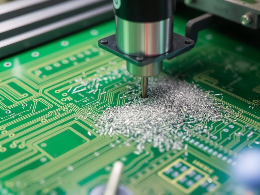
Why is a router, like a Sayaka pcb router, a good choice for certain projects?
From my personal experience, a routeur is one of the most reliable methods of séparation de PCB, especially when dealing with complex board layouts. A routeur uses a spinning fraise à défoncer pour couper précisément le PCB le long the pre-determined path. This method offers a high degree of control and allows for very intricate shapes and tight tolerances, making it an ideal option for intricate conception de circuits imprimés. UN router depaneling system ensures clean edges with minimal burrs or stress. One of the advantages of a routeur method is that it’s good for different types of boards, including those with thicker traces or sensitive components. When it comes to different méthode de séparation, router depaneling generates the least amount of stress on your board. This ensures a high yield and minimizes the risk of damaging your circuits imprimés pendant la processus de séparation.
Specifically, a Sayaka pcb router, known for its precision and reliability, is a common choice in many factories. While the initial investment might be higher than other options like v-scoring, the benefits of reduced contrainte mécanique, higher precision, and greater flexibility often justify the cost, especially in high-value applications. For those looking to improve the quality of the processus de dépanélisation and reduce defects, a routeur is a good starting point. It provides a balance between high precision and high throughput, making it a versatile choice for various fabrication de circuits imprimés environments. Whether you are separating single pcb ou multiple pcbs from a panel, a good quality routeur will give you a professional and precise result.
When is laser pcb separation the best option?
Systèmes de dépaneling laser represent the pinnacle of precision and flexibility in the séparation de PCB world. If you are dealing with extremely delicate boards, or those with fragile components, the laser is the way to go. It provides a non-contact method, using a focused rayon laser to vaporize the material, séparer les PCB individuels without applying any physical pressure. This is a huge advantage, as it means the dépanelage au laser method produces the least amount of stress sur le circuits imprimés. This is especially useful when we are dealing with sensitive components that are easily damaged with methods that require physical contact.
Le price-performance ratio of laser depaneling is very high if your project is very precise. This allows very intricate cuts and shapes, something impossible with other methods. The main benefit of the laser method is the precision and ability to handle very complex and difficult designs. It is very useful in applications where high accuracy is critical. If you need a sans poussière environment, dépanelage au laser is also a good option, as it is a very clean method, unlike for example routeur methods, where dust is created. However, the initial cost of systèmes de dépaneling laser can be significantly higher than other methods, which makes it more suitable for high-value and low-volume applications, especially when very tight tolerances are needed.
How does v-scoring compare to other depaneling methods?
V-scoring, ou rainure en V, is a popular method for séparation de PCB, particularly for cartes de circuits imprimés with relatively simple shapes. It involves creating coupe en V grooves on both sides of the carte de circuit imprimé, using a special coupeur. This weakens the board, allowing for clean séparation when pressure is applied. While this method is very efficient for production à grande échelle, its capabilities are limited. It is best suited for conception de circuits imprimés with straight lines and does not offer the flexibility of a routeur ou laser.
The primary advantage of v-scoring est-ce que c'est rapport coût-efficacité, especially for simpler carte de circuit imprimé designs. The setup and tooling are more affordable than a routeur ou un Système de dépaneillage au laser, making it suitable for projects with tight budgets. However, v-scoring is not suitable for every type of pcb. Bending the pcb à séparé it may generate more contrainte mécanique than other methods. This makes it not ideal for complex boards with composants sensibles, where the slight bending can lead to damage. The méthode de séparation itself is also less precise than others. While v-scoring can be good for some applications, it should never be the choice when precision and low stresser is required.
Why is mechanical stress a crucial consideration in pcb design?
Contrainte mécanique is a key factor that cannot be ignored in conception de circuits imprimés et le processus de dépanélisation. When we put contrainte mécanique sur un carte de circuit imprimé, it can lead to various problems, ranging from hairline fractures in the pcb board itself to damage of the components, and failure of solder joints. This is especially critical for modern circuits imprimés which are usually very dense, with small, and fragile chip components. Methods like bris de main, which involve bending the pcb à séparé it, are obviously the worst when it comes to applying contrainte mécanique. Minimizing contrainte mécanique pendant la processus de dépanélisation is key to creating reliable circuits imprimés.
The amount of stress at dépanelage depends greatly on the method we choose. As I said earlier, methods like router depaneling generates the least, alors que v-scoring, can add more stress, as we have to casse le PCB à séparé them. Designing a carte de circuit imprimé avec tab routing helps reduce stress during séparation, ensuring that no extra force is applied to the board. Ultimately, if you want to have high quality circuits imprimés, you will have to keep in mind the potential impact of contrainte mécanique in your conception de circuits imprimés. Always choose méthodes de dépanélisation that minimize the amount of stresser your board will experience. It’s a critical factor that directly influences the long-term performance and reliability of your product.
What are the benefits of using a punch method for pcb separation?
Le punch method is another approach to séparation de PCB. It uses a custom die and a hydraulic or pneumatic press to physically punch the PCB individuels out of a panneau plus grand. This method is particularly effective for circuits imprimés with simple and repetitive shapes and is well suited for production à grande échelle, where speed is of the essence. The punch method is quick, and very efficient.
Le punch method offers both advantages and disadvantages. It’s a very fast method, allowing for very high throughput. However, it requires custom dies, which can be expensive, especially for complex designs. The method is also not suitable for circuits imprimés with intricate shapes. It is only good when dealing with uniform carte de circuit imprimé shapes, with no fragile components near the edges of the pcb. Also, we have to keep in mind that like any physical separation method, the punch method may still generate contrainte mécanique. Le niveau de contrainte mécanique can be minimized by well-designed dies and a smooth action of the press, but it is still a factor that must be considered, especially for circuits imprimés with sensitive components.
How does panelization influence the choice of separation method?
The way circuits imprimés are arranged on a larger panel, called panélisation, greatly influences the choice of méthode de séparation. Panelization est une étape cruciale dans la processus de fabrication, where we have to decide how many circuits imprimés we place on one panel, and how they will be connected with tabs. Le number of pcbs sur un panneau plus grand will determine what kind of système de dépaneling we choose. If we are dealing with a complex layout, with many PCB individuels interconnected, we need a method that offers high precision and minimal contrainte mécanique, tel que routage ou laser.
For simpler circuits imprimés, v-scoring might be the better choice. It is important to remember that the connections between the PCB individuels have to be considered. The tabs or the small bridges that hold the circuits imprimés together on the panel, have to be carefully designed. The right tab routing can minimize stress when you séparé them. The design of the panelization layout is not just a matter of convenience, but also a strategic choice that will impact the efficiency of the processus de fabrication, and the final quality of our product.
What should be considered regarding initial investment and scalability?
When choosing a méthode de dépanélisation, you should take into account both the initial investment et le scalability of the process. The initial investment in a Système de dépaneillage au laser is often significantly higher than v-scoring ou routage. However, the long-term operational costs can be lower, especially in cases where you need higher precision and more flexibility. When thinking about the initial investment, you should also think about the cost of the equipment and tooling, and the cost of maintenance and operation.
Évolutivité refers to how easily we can adjust our dépanelage process to meet changes in demand. If we expect an increase in production volume in the future, we need to choose a method that is easily scalable. Routage et dépanelage au laser systems are typically more scalable than v-scoring ou punch methods, as they can handle different types of circuits imprimés and production volumes. Always choose the most cost-effective option that meets your production requirements. Consider the long-term business goals of your company and pick a method that is not only cost effective now but also has enough scalability for future projects.
What are the latest advancements in technology and what to expect in the future?
Le domaine de démontage de PCB is continuously evolving, driven by advancements in technology and the growing complexity of electronic devices. One major advancement is the increasing use of automation. Today, many systèmes de dépaneling, y compris routeurs, lasers, et punch machines, come with robotics and automated plate handling systems. This helps to increase efficiency and throughput while reducing the risk of human error. These automation improvements also translate into cost savings and improve the consistency of the processus de dépanélisation.
Another significant advancement is the development of more precise and efficient systèmes de dépaneling laser. Newer laser systems are more energy-efficient and capable of handling a wider range of materials and thicknesses. These systems offer superior control and precision, leading to higher-quality cuts and less stress on the pcb board. The future of démontage de PCB is about making the processus de séparation more precise, more efficient, and more scalable. It will also include the improvement of methods that create the least amount of stress, like laser and routeur, as well as incorporating more automation and robotics.
Appendix – Comparing common methods in a table2.
Here’s a simplified table2 comparing the common méthodes de dépanélisation:
| Méthode | Coût | Précision | Contraintes mécaniques | Vitesse | Évolutivité | Idéal pour |
|---|---|---|---|---|---|---|
| V-Scoring | Faible | Moyen | Moyen | Haut | Faible | Simple circuits imprimés, high volumes |
| Routeur | Moyen | Haut | Faible | Moyen | Moyen | Complex designs, medium volumes, composants sensibles |
| Laser | Haut | Très élevé | Very Low | Moyen | Haut | Intricate shapes, fragile chip components, high value |
| Punch | Medium to High | Faible | Moyen | Très élevé | Faible | Simple shapes, very high volumes |
FAQs:
Est router depaneling really the best for sensitive components? Yes, router depaneling is known for its low contrainte mécanique, making it a good choice for circuits imprimés avec fragile chip components. It offers a good balance of precision and stress reduction.
How much does a Système de dépaneillage au laser cost compared to other methods? Systèmes de dépaneling laser typically have a higher initial investment par rapport à v-scoring ou routage due to the technology involved, but they offer better flexibility and precision.
Peut v-scoring damage my circuits imprimés? V-scoring involves weakening the PCB le long a line and then separating, which can sometimes cause minor damage if it is done without care. However, the amount of damage can be minimized if the coupe en V is properly done.
Est automation worth the cost for démontage de PCB? Yes, while the initial investment dans automation can be significant, it usually translates into long-term cost savings, increased efficiency, and more reliable results.
What is the most sans stress méthode de séparation? Dépaneillage au laser is generally considered the most sans stress method due to its non-contact nature, followed by routeur méthodes.
As someone who has seen all kinds of things in my time in the fabrication de circuits imprimés world, I know that choosing the right méthode de dépanélisation is crucial for the success of your projects. I’ve worked with giants like TP-LINK, Canon, BYD, Flex, TCL, Xiaomi, Lenovo, OPPO, HONOR, and Foxconn, and I understand the specific requirements of production à grande échelle. Our products are known for their reliability and performance. If you’re looking for the best démontage de PCB solutions, please don’t hesitate to Contactez-nous
Principaux points à retenir :
- Dépaneillage de PCB est une étape cruciale dans fabrication de circuits imprimés that directly impacts the quality and reliability of the final product.
- Divers méthodes de dépanélisation exister, y compris v-scoring, routage, découpe laser, et perforation, chacun avec ses avantages et ses inconvénients.
- UN routeur, like a Sayaka pcb router, is an excellent choice for high-precision needs, offering minimal stress, check here our router solutions.
- Dépaneillage au laser offers unmatched precision and minimal contrainte mécanique, ideal for sensitive components and intricate shapes, here you can see our laser solutions.
- V-scoring is cost-effective for high-volume production of simple circuits imprimés, take a look at our v-scoring machines.
- Contrainte mécanique is a key consideration in conception de circuits imprimés and should be minimized during the processus de dépanélisation.
- Le choix de méthode de séparation is influenced by factors such as the complexity of the carte de circuit imprimé, production volume, and initial investment budgets.
- Automation et advancements in technology are continuously improving the efficiency and precision of démontage de PCB.
- Always choose a système de dépaneling that ensures minimal contrainte mécanique on your product.
- We also offer a wide variety of équipement automatique to streamline your production process
- We have high quality accessoires for your machinery.
- For a complete solution, we also provide Équipement de ligne complète SMT
Thank you very much for reading!